SNVSCF0 October 2024 LM65680-Q1
ADVANCE INFORMATION
- 1
- 1 Features
- 2 Applications
- 3 Description
- 4 Device Comparison Table
- 5 Pin Configuration and Functions
- 6 Specifications
-
7 Detailed Description
- 7.1 Overview
- 7.2 Functional Block Diagram
- 7.3
Feature Descriptions
- 7.3.1 Output Voltage Selection
- 7.3.2 EN Pin and Use as VIN UVLO
- 7.3.3 Device Configuration
- 7.3.4 Single-Output Dual-Phase Operation
- 7.3.5 Mode Selection
- 7.3.6 Adjustable Switching Frequency
- 7.3.7 Dual Random Spread Spectrum (DRSS)
- 7.3.8 Internal LDO, VCC UVLO, and BIAS Input
- 7.3.9 Bootstrap Voltage (BST Pin)
- 7.3.10 Soft Start and Recovery From Dropout
- 7.3.11 Safety Features
- 7.4 Device Functional Modes
- 8 Application and Implementation
- 9 Device and Documentation Support
- 10Revision History
- 11Mechanical, Packaging, and Orderable Information
Package Options
Mechanical Data (Package|Pins)
- RZY|26
Thermal pad, mechanical data (Package|Pins)
Orderable Information
7.3.7 Dual Random Spread Spectrum (DRSS)
| Observation | Root Cause | Recommendation |
|---|---|---|
| DRSS pin functionality is different between the prototype device and the final device. | Definition change based on the prototype results. See Table 7-5 and Table 7-4. | If DRSS disabled is a desired setting, connect a 49.9kΩ to GND on the DRSS pin to have the same device behavior when transitioning from the prototype device to the final device. |
| If DRSS enabled is a desired setting, tie the DRSS pin to the VCC pin to have a similar device behavior when transitioning from the prototype device to the final device. |
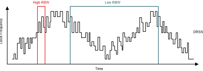
The LM656x0-Q1 provides a Dual Random Spread Spectrum (DRSS) function, which reduces EMI of the power supply over a wide-frequency range. The DRSS function combines a low-frequency triangular modulation profile with a high-frequency cycle-by-cycle pseudo-random modulation profile. The low frequency triangular modulation improves performance in the lower radio frequency bands, while the high frequency random modulation improves performance in the higher radio frequency bands.
As shown in Table 7-5, the two low frequency triangular modulation profiles are pin-selectable on the prototype device. The standard low-frequency modulation profile spreads the switching frequency by ±5% with a 12kHz modulation frequency while the wide low frequency modulation profile spreads the switching frequency by ±10% with a 6kHz modulation frequency. The slew rate control is always enabled on the prototype device.
As shown in Table 7-4, the final LM656x0-Q1 device provides a switch-node waveform shaping feature that, when enabled, adjusts the switch-node waveform rising transition for reduced ringing and overshoot. The final device provides the wide low frequency modulation profile which spreads the switching frequency by ±10% with a 6kHz modulation frequency.
| DRSS / MODECOMM Pin | DRSS | Slew Rate Control |
|---|---|---|
| Short to VCC(1) | Enabled, ±10%, 6kHz | Enabled |
| Float | Enabled, ±10%, 6kHz | Enabled |
| 150kΩ to GND | Enabled, ±10%, 6kHz | Disabled |
| 49.9kΩ to GND | Disabled | Enabled |
| Short to GND(1) | Disabled | Disabled |
| DRSS / MODECOMM Pin | DRSS | Slew Rate Control |
|---|---|---|
| Short to VCC(1) | Enabled, ±5%, 12kHz | Enabled |
| Float | Enabled, ±5%, 12kHz | Enabled |
| 150kΩ to GND | Enabled, ±10%, 6kHz | Enabled |
| 49.9kΩ to GND | Disabled | Enabled |
| Short to GND(1) | Disabled | Enabled |
Spread spectrum works by converting a narrowband signal into a wideband signal, which spreads the energy over multiple frequencies. Industry standards require different spectrum analyzer resolution bandwidth (RBW) settings for different frequency bands. The RBW has an impact on the spread spectrum performance. For example, the CISPR-25 requires 9kHz RBW for the 150kHz to 30MHz frequency band. For frequencies greater than 30MHz, the required RBW is 120kHz. DRSS is able to simultaneously improve the EMI performance in the high and low RBWs with the low frequency triangular modulation and high-frequency cycle-by-cycle pseudo-random modulation. In the low-frequency band (150kHz -30MHz), the DRSS function can reduce the conducted emissions by as much as 15dBμV, and in the high-frequency band (30MHz - 108MHz) by as much as 5dBμV. The DRSS function is disabled when an external clock is applied to the MODE/SYNC pin.
 Figure 7-7 Dual Random Spread Spectrum
Implementation