SBAS813 June   2018 ADS8688AT

PRODUCTION DATA.  

  1. Features
  2. Applications
  3. Description
  4. Revision History
  5. Pin Configuration and Functions
    1.     Pin Functions
  6. Specifications
    1. 6.1 Absolute Maximum Ratings
    2. 6.2 ESD Ratings
    3. 6.3 Recommended Operating Conditions
    4. 6.4 Thermal Information
    5. 6.5 Electrical Characteristics
    6. 6.6 Timing Requirements: Serial Interface
    7. 6.7 Switching Characteristics: Serial Interface
    8. 6.8 Typical Characteristics
  7. Detailed Description
    1. 7.1 Overview
    2. 7.2 Functional Block Diagram
    3. 7.3 Feature Description
      1. 7.3.1  Analog Inputs
      2. 7.3.2  Analog Input Impedance
      3. 7.3.3  Input Overvoltage Protection Circuit
      4. 7.3.4  Programmable Gain Amplifier (PGA)
      5. 7.3.5  Second-Order, Low-Pass Filter (LPF)
      6. 7.3.6  ADC Driver
      7. 7.3.7  Multiplexer (MUX)
      8. 7.3.8  Reference
        1. 7.3.8.1 Internal Reference
        2. 7.3.8.2 External Reference
      9. 7.3.9  Auxiliary Channel
        1. 7.3.9.1 Input Driver for the AUX Channel
      10. 7.3.10 ADC Transfer Function
      11. 7.3.11 Alarm Feature
    4. 7.4 Device Functional Modes
      1. 7.4.1 Device Interface
        1. 7.4.1.1 Digital Pin Description
          1. 7.4.1.1.1 CS (Input)
          2. 7.4.1.1.2 SCLK (Input)
          3. 7.4.1.1.3 SDI (Input)
          4. 7.4.1.1.4 SDO (Output)
          5. 7.4.1.1.5 DAISY (Input)
          6. 7.4.1.1.6 RST/PD (Input)
        2. 7.4.1.2 Data Acquisition Example
        3. 7.4.1.3 Host-to-Device Connection Topologies
          1. 7.4.1.3.1 Daisy-Chain Topology
          2. 7.4.1.3.2 Star Topology
      2. 7.4.2 Device Modes
        1. 7.4.2.1 Continued Operation in the Selected Mode (NO_OP)
        2. 7.4.2.2 Frame Abort Condition (FRAME_ABORT)
        3. 7.4.2.3 STANDBY Mode (STDBY)
        4. 7.4.2.4 Power-Down Mode (PWR_DN)
        5. 7.4.2.5 Auto Channel Enable With Reset (AUTO_RST)
        6. 7.4.2.6 Manual Channel n Select (MAN_Ch_n)
        7. 7.4.2.7 Channel Sequencing Modes
        8. 7.4.2.8 Reset Program Registers (RST)
    5. 7.5 Register Maps
      1. 7.5.1 Command Register Description
      2. 7.5.2 Program Register Description
        1. 7.5.2.1 Program Register Read/Write Operation
        2. 7.5.2.2 Program Register Map
        3. 7.5.2.3 Program Register Descriptions
          1. 7.5.2.3.1 Auto-Scan Sequencing Control Registers
            1. 7.5.2.3.1.1 Auto-Scan Sequence Enable Register (address = 01h)
              1. Table 11. AUTO_SEQ_EN Field Descriptions
            2. 7.5.2.3.1.2 Channel Power Down Register (address = 02h)
              1. Table 12. Channel Power Down Register Field Descriptions
          2. 7.5.2.3.2 Device Features Selection Control Register (address = 03h)
            1. Table 13. Feature Select Register Field Descriptions
          3. 7.5.2.3.3 Range Select Registers (addresses 05h-0Ch)
            1. Table 16. Channel n Input Range Registers Field Descriptions
          4. 7.5.2.3.4 Alarm Flag Registers (Read-Only)
            1. 7.5.2.3.4.1 ALARM Overview Tripped-Flag Register (address = 10h)
              1. Table 17. ALARM Overview Tripped-Flag Register Field Descriptions
            2. 7.5.2.3.4.2 Alarm Flag Registers: Tripped and Active (address = 11h to 14h)
              1. Table 18. ALARM Ch0-3 Tripped-Flag Register Field Descriptions
              2. Table 19. ALARM Ch0-3 Active-Flag Register Field Descriptions
              3. Table 20. ALARM Ch4-7 Tripped-Flag Register Field Descriptions
              4. Table 21. ALARM Ch4-7 Active-Flag Register Field Descriptions
          5. 7.5.2.3.5 Alarm Threshold Setting Registers
            1. Table 22. Channel n Hysteresis Register Field Descriptions (n = 0 to 7)
            2. Table 23. Channel n High Threshold MSB Register Field Descriptions (n = 0 to 7)
            3. Table 24. Channel n High Threshold LSB Register Field Descriptions (n = 0 to 7)
            4. Table 25. Channel n Low Threshold MSB Register Field Descriptions (n = 0 to 7)
            5. Table 26. Channel n Low Threshold MSB Register Field Descriptions (n = 0 to 7)
          6. 7.5.2.3.6 Command Read-Back Register (address = 3Fh)
            1. Table 27. Command Read-Back Register Field Descriptions
  8. Application and Implementation
    1. 8.1 Application Information
    2. 8.2 Typical Applications
      1. 8.2.1 Phase-Compensated, 8-Channel, Multiplexed Data Acquisition System for Power Automation
        1. 8.2.1.1 Design Requirements
        2. 8.2.1.2 Detailed Design Procedure
        3. 8.2.1.3 Application Curve
      2. 8.2.2 16-Bit, 8-Channel, Integrated Analog Input Module for Programmable Logic Controllers (PLCs)
        1. 8.2.2.1 Design Requirements
        2. 8.2.2.2 Detailed Design Procedure
        3. 8.2.2.3 Application Curve
  9. Power Supply Recommendations
  10. 10Layout
    1. 10.1 Layout Guidelines
    2. 10.2 Layout Example
  11. 11Device and Documentation Support
    1. 11.1 Documentation Support
      1. 11.1.1 Related Documentation
    2. 11.2 Receiving Notification of Documentation Updates
    3. 11.3 Community Resources
    4. 11.4 Trademarks
    5. 11.5 Electrostatic Discharge Caution
    6. 11.6 Glossary
  12. 12Mechanical, Packaging, and Orderable Information

Package Options

Mechanical Data (Package|Pins)
Thermal pad, mechanical data (Package|Pins)
Orderable Information

Features

  • 16-Bit ADC With Integrated Analog Front-End
  • 8-Channel MUX With Auto and Manual Scan
  • Channel-Independent Programmable Inputs:
    • ±10.24 V, ±5.12 V, ±2.56 V, ±1.28 V, ±0.64 V
    • 10.24 V, 5.12 V, 2.56 V, 1.28 V
  • 5-V Analog Supply: 1.65-V to 5-V I/O Supply
  • Constant Resistive Input Impedance: 1 MΩ
  • Input Overvoltage Protection: Up to ±20 V
  • Integrated 4.096-V Reference With 6 ppm/°C Drift
  • Excellent Performance:
    • 500-kSPS Aggregate Throughput
    • DNL: ±0.5 LSB; INL: ±0.75 LSB
    • 1-ppm/°C Drift for Gain Error and Offset
    • SNR: 92 dB; THD: –102 dB
    • Low Power: 65 mW
  • AUX Input → Direct Connection to ADC Inputs
  • ALARM → High and Low Thresholds per Channel
  • SPI™-Compatible Interface With Daisy-Chain
  • Temperature Range: –55°C to +125°C
  • TSSOP-38 Package (9.7 mm × 4.4 mm)
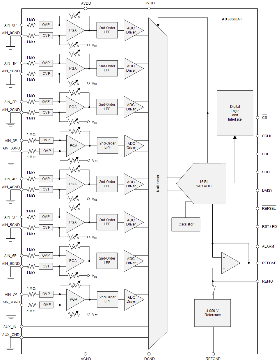
  • Block Diagram

    ADS8688AT frontpage_ads8688AT_sbas813.gif