SNOSDJ7A February 2025 – December 2025 LMG3650R025
PRODMIX
- 1
- 1 Features
- 2 Applications
- 3 Description
- 4 Pin Configuration and Functions
- 5 Specifications
- 6 Parameter Measurement Information
-
7 Detailed Description
- 7.1 Overview
- 7.2 Functional Block Diagram
- 7.3
Feature Description
- 7.3.1 Drive Strength Adjustment
- 7.3.2 GaN Power FET Switching Capability
- 7.3.3 VDD Supply
- 7.3.4 Overcurrent and Short-Circuit Protection
- 7.3.5 Overtemperature Protection
- 7.3.6 UVLO Protection
- 7.3.7 Fault Reporting
- 7.3.8 Auxiliary LDO (LMG3651R025 Only)
- 7.3.9 Zero-Voltage Detection (ZVD) (LMG3656R025 Only)
- 7.4 Device Functional Modes
- 8 Application and Implementation
- 9 Device and Documentation Support
- 10Revision History
- 11Mechanical, Packaging, and Orderable Information
8.4.2 Layout Example
Correct layout of the LMG365xR025 and surrounding components is essential for correct operation.
The layouts shown here reflect the GaN device schematic in Figure 8-1. The layouts in Figure 8-1 produce good results and are intended as a guideline. However, obtaining acceptable
performance with alternate layout schemes is possible. Additionally, please refer to the
land pattern example in Section 11.2 for the latest recommended PCB footprint of the device.
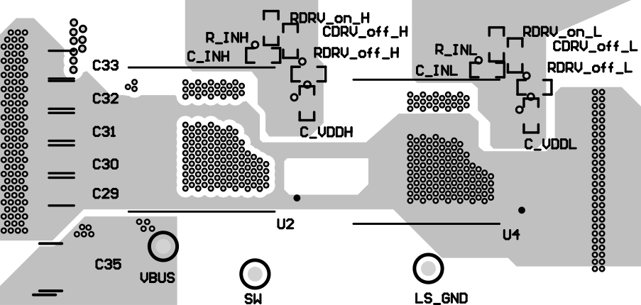
 Figure 8-12 LMG3650R025
Half-Bridge Top-Layer Layout
 Figure 8-13 LMG3650R025
Half-Bridge Mid-Layer Layout
The top-layer layout and mid-layer layout are shown. The layouts are zoomed in to the LMG3650R025 U2 and U4 component placements. The mid-layer layout includes the outlines of the top layer components to assist the user in lining up the top-layer and mid-layer layouts.
 Figure 8-12 LMG3650R025
Half-Bridge Top-Layer Layout
 Figure 8-13 LMG3650R025
Half-Bridge Mid-Layer Layout