SPRACM3E August 2021 – January 2023 F29H850TU , F29H859TU-Q1 , TMS320F280021 , TMS320F280021-Q1 , TMS320F280023 , TMS320F280023-Q1 , TMS320F280023C , TMS320F280025 , TMS320F280025-Q1 , TMS320F280025C , TMS320F280025C-Q1 , TMS320F280033 , TMS320F280034 , TMS320F280034-Q1 , TMS320F280036-Q1 , TMS320F280036C-Q1 , TMS320F280037 , TMS320F280037-Q1 , TMS320F280037C , TMS320F280037C-Q1 , TMS320F280038-Q1 , TMS320F280038C-Q1 , TMS320F280039 , TMS320F280039-Q1 , TMS320F280039C , TMS320F280039C-Q1 , TMS320F280040-Q1 , TMS320F280040C-Q1 , TMS320F280041 , TMS320F280041-Q1 , TMS320F280041C , TMS320F280041C-Q1 , TMS320F280045 , TMS320F280048-Q1 , TMS320F280048C-Q1 , TMS320F280049 , TMS320F280049-Q1 , TMS320F280049C , TMS320F280049C-Q1 , TMS320F28384D , TMS320F28384S , TMS320F28386D , TMS320F28386S , TMS320F28388D , TMS320F28388S , TMS320F28P650DH , TMS320F28P650DK , TMS320F28P650SH , TMS320F28P650SK , TMS320F28P659DH-Q1 , TMS320F28P659DK-Q1 , TMS320F28P659SH-Q1
- Using the Fast Serial Interface (FSI) With Multiple Devices in an Application
- Trademarks
- 1Introduction to the FSI Module
- 2FSI Applications
- 3Handshake Mechanism
- 4Sending and Receiving FSI Data Frames
- 5Daisy-Chain Topology Tests
- 6Star Topology Tests
-
7Event Synchronization Over FSI
- 7.1 Introduction
- 7.2 C2000Ware FSI EPWM Sync Examples
- 7.3 Additional Tips and Usage of FSI Event Sync
- 8References
- 9Revision History
5.1.2 DMA Control
- Test condition
Device 1 sends data -> Device 2 receives data -> Device 2 DMA moves RX data to TX buffer and registers -> Device 2 triggers TX when TX_FRAME_TAG_UDATA FSI register is written to which forwards the received data back to Device 1 -> Device 1 receives data back -> Device 1 DMA moves RX data to memory -> CPU verifies data in memory matches the originally sent TX data.
- Test case
Data length of 8 words (8 words per burst, 1 burst per transfer), two data lines, TXCLK = 50 MHz, with Setting ② (Table 5-1) enabled.
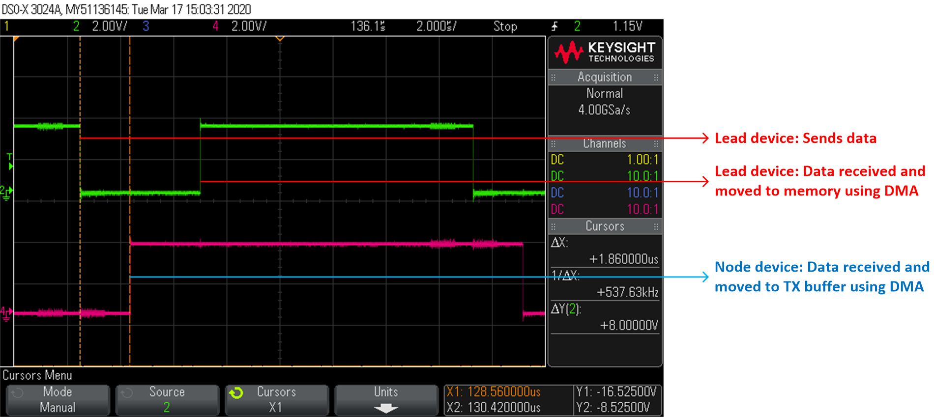
In this test, DMA interrupts from CH2 and CH4 are enabled to trigger at the end of a transfer in the lead device, which means that interrupts occur every time data has been copied from memory to the FSITX buffer (CH2) or data has been transferred out of the FSRX buffer to a location in memory (CH4). In the node device, the DMA channels are configured to transfer received data from the RX buffers and registers to the TX buffers and registers anytime an FSI data frame is received, ultimately forwarding the data back to the lead device. Therefore the node device only has one DMA interrupt enabled while the lead device has two. With GPIOs toggling in the DMA ISRs, Figure 5-4 shows the test results of FSI communication using DMA control.
 Figure 5-4 FSI Communication Using DMA
Control
Figure 5-4 FSI Communication Using DMA
ControlIt should be noted that the time of 1.86 µs shown includes the time for the lead device to transmit the data frame, the node device to move RX data to the TX buffer / registers, entering of the ISR, and toggling the GPIO. According to the DMA pipeline timing requirements (See device specific TRM referenced in Section 8 for more info), the time for moving data of 9 words (8 words data + 1 word of user data and frame tag) using 2 channels can be calculated as shown in Equation 2.
Thus, considering other delay times, the actual transmission time is almost aligned with the former test result (1.4 µs) using CPU control. Also, it should be highlighted that utilizing the DMA in this case drastically saves the time for transferring received data, especially in an application with mass data transmissions..