SPRACM3E August 2021 – January 2023 F29H850TU , F29H859TU-Q1 , TMS320F280021 , TMS320F280021-Q1 , TMS320F280023 , TMS320F280023-Q1 , TMS320F280023C , TMS320F280025 , TMS320F280025-Q1 , TMS320F280025C , TMS320F280025C-Q1 , TMS320F280033 , TMS320F280034 , TMS320F280034-Q1 , TMS320F280036-Q1 , TMS320F280036C-Q1 , TMS320F280037 , TMS320F280037-Q1 , TMS320F280037C , TMS320F280037C-Q1 , TMS320F280038-Q1 , TMS320F280038C-Q1 , TMS320F280039 , TMS320F280039-Q1 , TMS320F280039C , TMS320F280039C-Q1 , TMS320F280040-Q1 , TMS320F280040C-Q1 , TMS320F280041 , TMS320F280041-Q1 , TMS320F280041C , TMS320F280041C-Q1 , TMS320F280045 , TMS320F280048-Q1 , TMS320F280048C-Q1 , TMS320F280049 , TMS320F280049-Q1 , TMS320F280049C , TMS320F280049C-Q1 , TMS320F28384D , TMS320F28384S , TMS320F28386D , TMS320F28386S , TMS320F28388D , TMS320F28388S , TMS320F28P650DH , TMS320F28P650DK , TMS320F28P650SH , TMS320F28P650SK , TMS320F28P659DH-Q1 , TMS320F28P659DK-Q1 , TMS320F28P659SH-Q1
- Using the Fast Serial Interface (FSI) With Multiple Devices in an Application
- Trademarks
- 1Introduction to the FSI Module
- 2FSI Applications
- 3Handshake Mechanism
- 4Sending and Receiving FSI Data Frames
- 5Daisy-Chain Topology Tests
- 6Star Topology Tests
-
7Event Synchronization Over FSI
- 7.1 Introduction
- 7.2 C2000Ware FSI EPWM Sync Examples
- 7.3 Additional Tips and Usage of FSI Event Sync
- 8References
- 9Revision History
1 Introduction to the FSI Module
The FSI module is a serial communication peripheral capable of reliable and robust high-speed communications, up to 200 Mbps. Utilizing very few unidirectional signals, FSI provides a low cost way of communicating across an isolation barrier when leveraging digital isolation devices. Thus, FSI enables new ways of distributing the powerful sensing, processing, and actuation capabilities of C2000 MCUs in industrial applications, where real-time control with critical communication speed is required.
Generally, FSI can be implemented in two kinds of system conditions:
- Wired communications between MCUs that exist on the same voltage and ground planes.
- Wired communications across an isolation barrier, leveraging digital isolators (like ISO77xx), commonly used for MCUs placed on the hot-side needing to communicate with MCUs on the cold-side, or between boards with different voltage and ground planes.
There are a number of real-time systems that can benefit from the FSI peripheral. A multi-axis servo drive can be constructed with C2000 device nodes controlling each axis. Having FSI serve as the communication link, control loop information can be quickly transmitted and received between the devices to maintain precise motion control. For an example of this system see the Distributed Multi-axis Servo Drive over Fast Serial Interface (FSI) reference design.
Additionally, with increasing global power consumption, the need for higher efficiency power supplies, in conjunction with the availability of wide bandgap GaN and SiC products, is driving the use of more sophisticated power distribution architectures. Decentralized power control solutions using C2000 MCUs can be connected and made flexible with FSI to meet these requirements. For a discussion on such power related systems see the Distributed Power Control Architecture with Multiple MCUs Over FSI.
The FSI peripheral offers a broad range of features, including programmable data length, hardware managed CRC, ECC support, and more. A PING watchdog and Frame watchdog can enable automatic line-break detection. The unique delay line control feature implemented within the FSI receive module can adjust for channel-to-channel skew introduced by trace-length mismatch, transceivers, or digital isolation ICs, allowing FSI to maintain high-speed and robust communication.
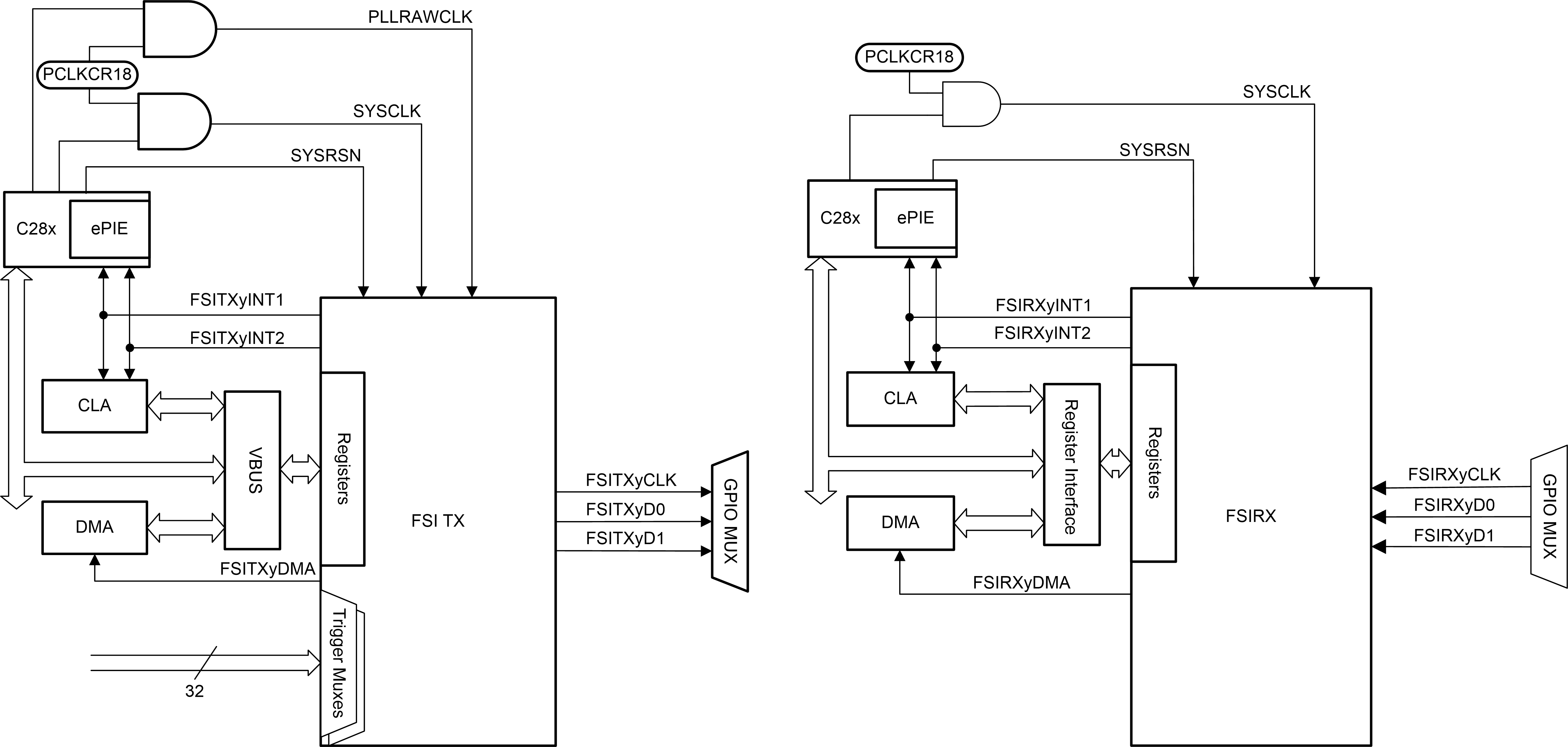
The FSI consists of the independent transmitter (FSITX) and receiver (FSIRX) cores, which are configured and operated independently. Because of this, the FSI protocol does not have a notion of master and slave, unlike some other synchronous communication protocols, and allows for simultaneous full speed communications in both directions. Figure 1-1 shows the CPU interface of each FSI module. Each module owns up to three signal lines: one clock and two data signals, where the second data lines, FSITXyD1 and FSIRXyD1, are optional, and can be enabled for multi-lane transmission and double the speed for data bits. Thus, at least four signal lines are needed to create 2-way point-to-point communication. Considering the timing spec for FSITX (see the device-specific data sheets referenced in Section 8), the maximum data rate of 200 Mbps can be achieved with the maximum clock of 50 MHz, using two data lines, since the data is transmitted on both edges of the clock signal. For a full overview of FSI including all features and functions available, see the device-specific Technical Reference Manual (TRM).
 Figure 1-1 FSITX and FSIRX CPU Interface