SPRACM3E August 2021 – January 2023 F29H850TU , F29H859TU-Q1 , TMS320F280021 , TMS320F280021-Q1 , TMS320F280023 , TMS320F280023-Q1 , TMS320F280023C , TMS320F280025 , TMS320F280025-Q1 , TMS320F280025C , TMS320F280025C-Q1 , TMS320F280033 , TMS320F280034 , TMS320F280034-Q1 , TMS320F280036-Q1 , TMS320F280036C-Q1 , TMS320F280037 , TMS320F280037-Q1 , TMS320F280037C , TMS320F280037C-Q1 , TMS320F280038-Q1 , TMS320F280038C-Q1 , TMS320F280039 , TMS320F280039-Q1 , TMS320F280039C , TMS320F280039C-Q1 , TMS320F280040-Q1 , TMS320F280040C-Q1 , TMS320F280041 , TMS320F280041-Q1 , TMS320F280041C , TMS320F280041C-Q1 , TMS320F280045 , TMS320F280048-Q1 , TMS320F280048C-Q1 , TMS320F280049 , TMS320F280049-Q1 , TMS320F280049C , TMS320F280049C-Q1 , TMS320F28384D , TMS320F28384S , TMS320F28386D , TMS320F28386S , TMS320F28388D , TMS320F28388S , TMS320F28P650DH , TMS320F28P650DK , TMS320F28P650SH , TMS320F28P650SK , TMS320F28P659DH-Q1 , TMS320F28P659DK-Q1 , TMS320F28P659SH-Q1
- Using the Fast Serial Interface (FSI) With Multiple Devices in an Application
- Trademarks
- 1Introduction to the FSI Module
- 2FSI Applications
- 3Handshake Mechanism
- 4Sending and Receiving FSI Data Frames
- 5Daisy-Chain Topology Tests
- 6Star Topology Tests
-
7Event Synchronization Over FSI
- 7.1 Introduction
- 7.2 C2000Ware FSI EPWM Sync Examples
- 7.3 Additional Tips and Usage of FSI Event Sync
- 8References
- 9Revision History
5.1.1 CPU Control
- Test condition
Device 1 sends data -> Device 2 receives data -> Device 2 CPU moves RX data to TX buffer and registers -> Device 2 triggers FSI TX with SW which forwards the received data back to Device 1 -> Device1 receives data back and the CPU verifies it matches the originally sent TX data.
- Test case
Data length of 8 words, two data lines, TXCLK = 50 MHz, with Setting ① (Table 5-1) enabled.
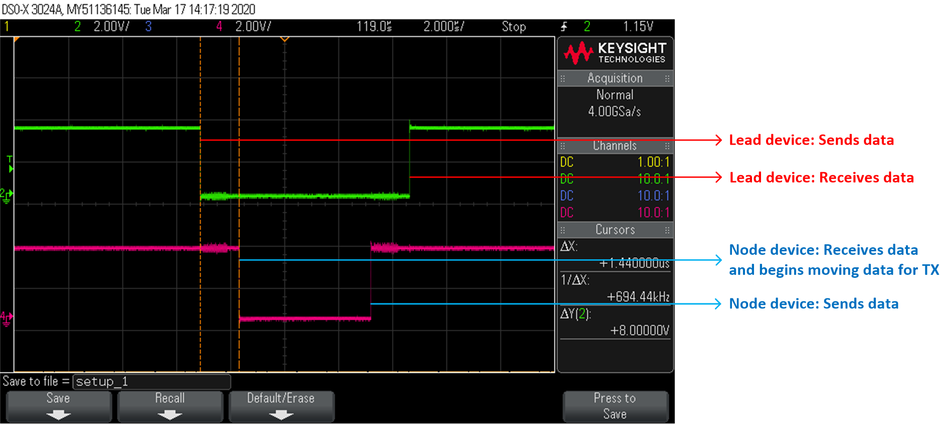
In the test, general-purpose input/output (GPIO)s are toggled within software when specific events occur during the communication and measured using an oscilloscope to obtain the respective timing data. In Figure 5-3, the green signal represents the GPIO toggling of Device 1 (Lead device) and the magenta signal represents the GPIO toggling of Device 2 (Node device).
 Figure 5-3 Data Transmission Test Using
CPU Control
Figure 5-3 Data Transmission Test Using
CPU ControlFrom the results shown in Figure 5-3, the time obtained for the data transmission is ~1.4 µs. In order to calculate the transmission speed, the total data length should be considered. Table 5-2 shows the general structure of a data frame, which can be divided into two parts: effective data bits and overhead bits.
- Effective Data Bits: Includes the 8-bit User Data, 16-bit Data Words, and 8-bit CRC fields
- Overhead Bits: Includes the Preamble, SOF, Frame Type, EOF, and Postamble fields
Therefore, the ideal transmission time for 8 words can be derived theoretically, as shown in Table 5-3.
It should be noted that since two data lines only work for effective data bits, one FSITXCLK cycle delivers 4 effective data bits, while one FSITXCLK cycle only delivers 2 overhead bits. Thus, with a total 48 FSITXCLK cycles for 8 data words, the transmission time can be calculated as shown in Equation 1.
Therefore, the theoretical transmission speed is 175 Mbps (168/0.96 µs), while the speed from the test is 120 Mbps with 1.4 µs transmission time, due to the fact that the tested transmission time includes entering the ISR (to toggle an IO pin), delay introduced by isolators, transceivers, cables, and so forth. If changing to one data line, the theoretical transmission speed is 100 Mbps, while the test speed is 80 Mbps with a transmission time of 2.1 µs.
Another finding from Figure 5-3 is that moving data from the FSIRX buffers to the FSITX buffers in the node device takes some time, approximately 4.9 µs using the FSI driverLib functions. This will be a key factor that distinguishes DMA and HW controls as shown in the next sections.
| IDLE | Preamble | SOF | Frame Type | User Data | Data Words | CRC | Frame Tag | EOF | Postamble | IDLE |
|---|---|---|---|---|---|---|---|---|---|---|
| 1111 | 1001 | 0011 | 8 bits | N words | 8 bits | 4 bits | 0110 | 1111 |
| Effective Data Bits (bits) | Overhead Bits (bits) | Total Length (bits) | FSITXCLK Cycles for Effective Data Bits (cycles) | FSITXCLK Cycles for Overhead Bits (cycles) | Total Data Transmission Time (us) |
|---|---|---|---|---|---|
| 144 | 24 | 168 | 36 | 12 | 0.96 |