SPRACM3E August 2021 – January 2023 F29H850TU , F29H859TU-Q1 , TMS320F280021 , TMS320F280021-Q1 , TMS320F280023 , TMS320F280023-Q1 , TMS320F280023C , TMS320F280025 , TMS320F280025-Q1 , TMS320F280025C , TMS320F280025C-Q1 , TMS320F280033 , TMS320F280034 , TMS320F280034-Q1 , TMS320F280036-Q1 , TMS320F280036C-Q1 , TMS320F280037 , TMS320F280037-Q1 , TMS320F280037C , TMS320F280037C-Q1 , TMS320F280038-Q1 , TMS320F280038C-Q1 , TMS320F280039 , TMS320F280039-Q1 , TMS320F280039C , TMS320F280039C-Q1 , TMS320F280040-Q1 , TMS320F280040C-Q1 , TMS320F280041 , TMS320F280041-Q1 , TMS320F280041C , TMS320F280041C-Q1 , TMS320F280045 , TMS320F280048-Q1 , TMS320F280048C-Q1 , TMS320F280049 , TMS320F280049-Q1 , TMS320F280049C , TMS320F280049C-Q1 , TMS320F28384D , TMS320F28384S , TMS320F28386D , TMS320F28386S , TMS320F28388D , TMS320F28388S , TMS320F28P650DH , TMS320F28P650DK , TMS320F28P650SH , TMS320F28P650SK , TMS320F28P659DH-Q1 , TMS320F28P659DK-Q1 , TMS320F28P659SH-Q1
- Using the Fast Serial Interface (FSI) With Multiple Devices in an Application
- Trademarks
- 1Introduction to the FSI Module
- 2FSI Applications
- 3Handshake Mechanism
- 4Sending and Receiving FSI Data Frames
- 5Daisy-Chain Topology Tests
- 6Star Topology Tests
-
7Event Synchronization Over FSI
- 7.1 Introduction
- 7.2 C2000Ware FSI EPWM Sync Examples
- 7.3 Additional Tips and Usage of FSI Event Sync
- 8References
- 9Revision History
5.2.2.1.2 Hardware Control
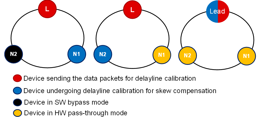
With hardware control case considered in the example, the Device 2 and Device 3 are always in hardware pass-through mode and so for skew compensation algorithm these devices have also to be in the pass-through mode.
Device 2 delayline calibration: The Device 1 calls the Device 2 using the assigned ID and once the Device 2 receives the calibration call, it uses the data packets sent by Device 1 to calibrate its delaylines. The Device 3, while in by-pass mode, transmits the packet received from the Device 2 to the Device 1 using CPU control.
Device 3 delayline calibration: The Device 1 calls the Device 3 using the assigned ID and once the Device 3 receives the calibration call, it uses the data packets sent by Device 1 to calibrate its delaylines. The Device 2, while in by-pass mode, transmits the packet received from the Device 1 to the Device 3 using the hardware channel that was previously calibrated.
Device 1 delayline calibration: Once the calibrations of Device 2 and Device 3 delaylines are completed, they go into by-pass mode where the received packets are transmitted via the hardware channels of each of the devices. With this configuration, the Device 1 starts calibrating its delaylines by sending data packets which return to its Rx. This way, effectively, the Device 1 is calibrating itself in an external loopback network where the loop is completed by the hardware channels of Device 2 and Device 3.
All the three devices are thus calibrated in a phased manner as shown in the figure Figure 5-14 and by the end of calibration the Rx delaylines of all the devices in the daisy chain are configured with appropriate values.
 Figure 5-14 Calibration Diagram of Delay
Lines for Skew Compensation in Hardware Control
Figure 5-14 Calibration Diagram of Delay
Lines for Skew Compensation in Hardware ControlThe below table lists the different functions used to build the skew compensation algorithm for the three-device daisy chain system. As noted earlier, the skew compensation algorithm is built-off of the existing examples in Fast Serial Interface (FSI) Skew Compensation and Table 5-6provides only those functions created for the purposes of skew compensation in daisy chain topology.
| Function | Description |
|---|---|
FSI_LpbkvalidatePing |
Used by the lead device to transmit and receive ping packets to validate the provided delayline configuration for skew compensation. This function expects the rest of the devices of the daisychain to be in loopback mode. |
FSI_LpbkCalibrateExePoint |
This function calls FSI_LpbkvalidatePing function for each possible configuration of the three delaylines of lead Rx and determines the best possible configuration for optimal skew compensation. This function expects the rest of the devices of the daisychain to be in loopback mode. |
Note that in case Device 2 and Device 3 should also transmit, the above skew compensation algorithm has to be extended such that the delay lines present on the Tx clock and data lines of these devices are calibrated by keeping the calibrated Rx delaylines of the system intact.