SPRADC3 june 2023 AM2431 , AM2432 , AM2434 , AM2631 , AM2631-Q1 , AM2632 , AM2632-Q1 , AM2634 , AM2634-Q1 , AM263P2 , AM263P2-Q1 , AM263P4 , AM263P4-Q1 , AM3351 , AM3352 , AM3354 , AM3356 , AM3357 , AM3358 , AM3358-EP , AM3359 , AM4372 , AM4376 , AM4377 , AM4378 , AM4379 , AM5706 , AM5708 , AM5716 , AM5718 , AM5718-HIREL , AM5726 , AM5728 , AM5729 , AM5746 , AM5748 , AM5749 , AM6411 , AM6412 , AM6421 , AM6422 , AM6441 , AM6442 , AM6526 , AM6528 , AM6546 , AM6548
3.1 PRU CRC16/32 Module
Cyclic redundancy check (CRC) is required in the communication frame package to ensure data accuracy during data transmission. Each PRU core has a designated peripheral CRC16/32 module to provide error detection capability to communication systems. CRC16/32 modules support features for CRC32, CRC16, and CRC16-CCITT with different polynomials. The module also connects with the PRU internal register R25 to R29 through use of the PRU broadside interface. R29 is mapping to the CRC_DATA register, supporting a maximum of 32-bit data widths and reads back checked data either as 16-bits or 32-bits, depending on the configuration. The 16-bit CRC data with 16-bit data words can be generated and put into each frame. Figure 3-1 shows the block diagram of the PRU CRC16/32 module and the following code demonstrates the CRC16 function for 16-bit data:
zero &r25, 4              ; config CRC type
xout CRC_XID, &25, 4      ; enable CRC module, CRC_XID = 0x1
mov  r29, r20             ; load CRC data, ASCII equivalent for "21"
xout CRC_XID, &29.w0, 2   ; push CRC data to CRC16 module
nop
xin  CRC_XID, &r28, 4     ; load the accumulated CRC result into PRU
Figure 3-1 PRU CRC16/32 Module Block
Diagram
Figure 3-1 PRU CRC16/32 Module Block
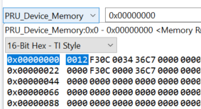
DiagramThe CRC input data must be swapped bytes, since the PRU is based on Least Significant Byte (LSByte)-first architecture. As an example, 0x3412 has to be given as the input data to perform CRC16 for 0x1234. Figure 3-2 shows the verification results for the CRC16/32 module. PRU0 receives data from thePRU1 GPO every 16 bits and stores in PRU DRAM from address 0x00000000.
The base address stores the raw data (0x12) sent by the PRU1 GPO. The received data is sent to the PRU0 CRC module and loads the accumulated CRC results into both the PRU0 R28 register and the memory address with an offset of 0x24. The memory address with offset 0x02 stores the CRC16 results (0xf30c) for data 0x12 from PRU1. Address offset 0x04 stores the raw data (0x34) sent by PRU1 GPO. The received data is sent to the PRU0 CRC module and loads the accumulated CRC results into both the PRU0 R28 register and memory address with offset 0x26. The memory address with offset 0x06 stores the CRC16 results (0x36c7) for data 0x34 from PRU1. Figure 3-2shows that from the memory values, both the raw data and CRC data are correct.
 Figure 3-2 PRU CRC16 Module
Verification