TIDA029A july 2019 – june 2023 CC2640R2F-Q1 , CC2642R , CC2642R-Q1
- 1
- Bluetooth Angle of Arrival (AoA) Antenna Design
- Trademarks
- 1Introduction
- 2Angle of Arrival Antenna Design Considerations
- 3Dipole Antenna Array
- 4Calculating AoA From IQ Measurements
- 5References
- 6Revision History
3.3 PCB Implementation
The ¼ λ dipole antennas were designed at the center of the Bluetooth Low Energy frequency spectrum (2.44 GHz) and therefore, have a length of about 30.8 mm. Notice that the phase centers are spaced 35 mm apart meeting the needed < ½ λ spacing requirement.
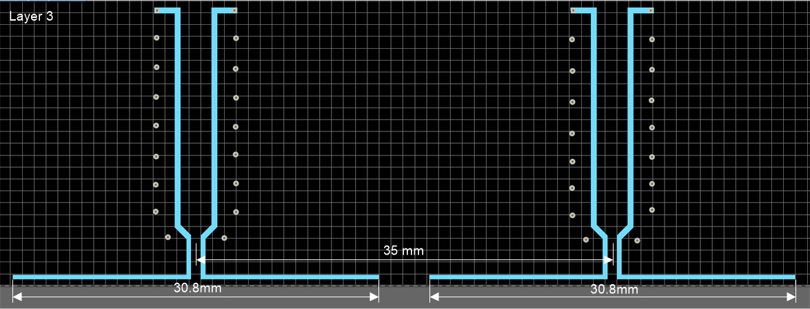 Figure 3-6 Layer 3 Dipole Spacing and
Width
Figure 3-6 Layer 3 Dipole Spacing and
WidthTo transform the balanced (differential) signal to an unbalanced (single-ended) signal, a PCB Marchand balun was implemented on the layer below the dipole antenna (layer 4).
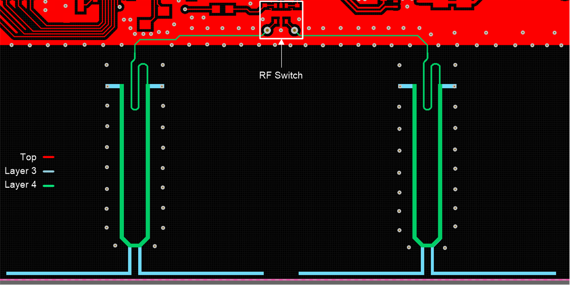 Figure 3-7 Layer 4 Marchand Balun
The Marchand balun was designed, simulated, and tested to ensure proper performance. The top section of the balun routed to the RF switch is used to match the 50-Ω impedance transmission line. Additionally, the board stack-up ensures proper spacing between the 3rd layer (dipole antenna) and the 4th layer (Marchand balun) for the correct amount of capacitive coupling between the two layers. Because the single-ended trace from the RF switch requires ground, the Marchand balun and dipole antenna feed traces are sandwiched between two identical ground planes, one on the 2nd layer and one on the 5th layer, as Figure 3-8 shows.
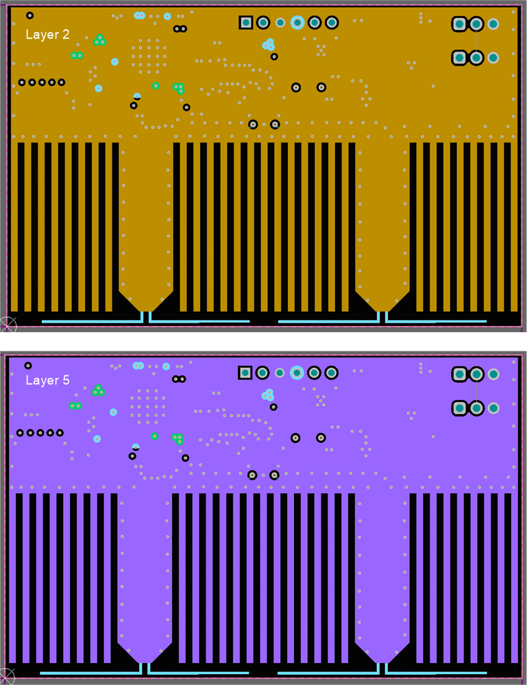 Figure 3-8 Layer 2 and 5 Ground
Planes
Figure 3-8 Layer 2 and 5 Ground
PlanesFigure 3-9 through Figure 3-12 show the dimensions for the dipole antennas, Marchand balun, and GND planes.
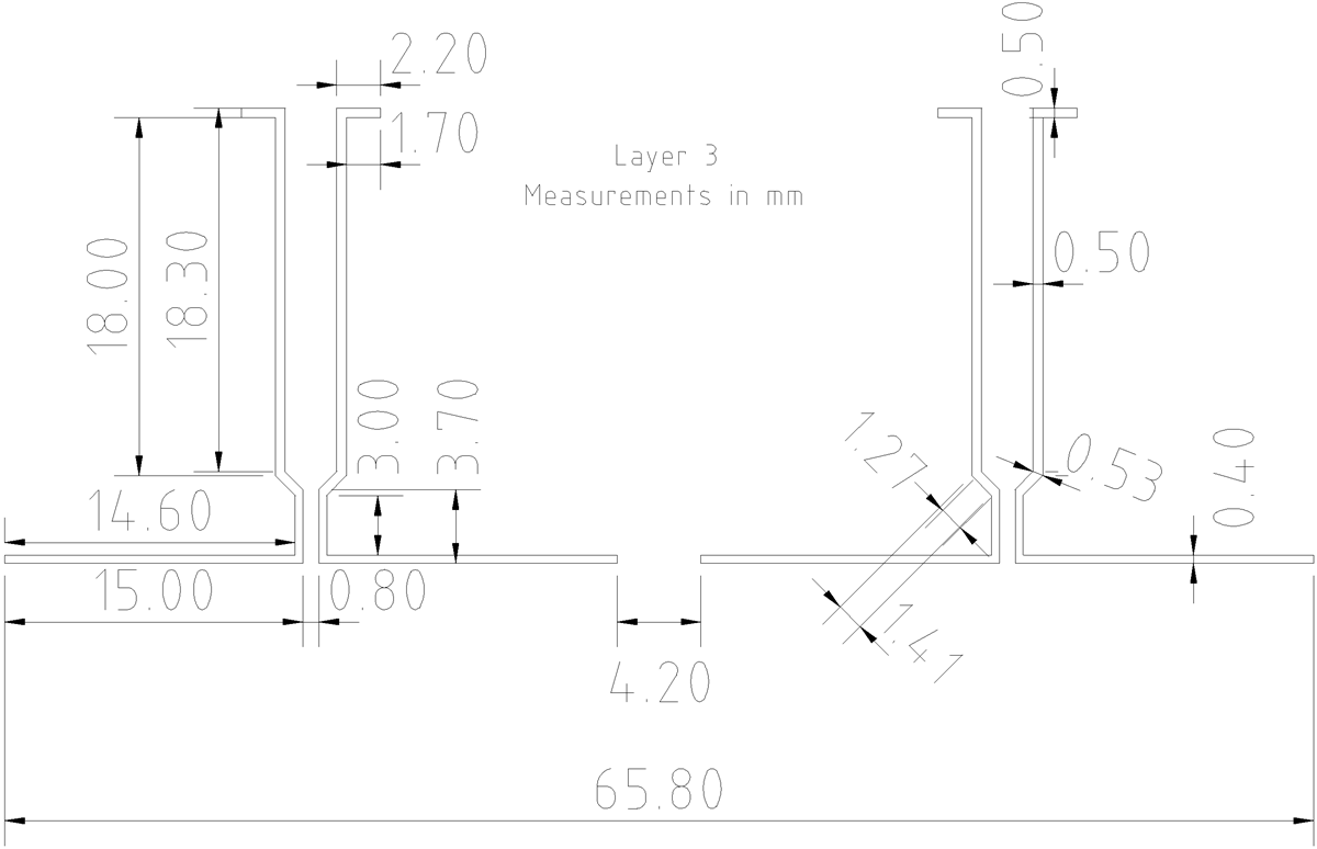 Figure 3-9 Layer 3 Dipole Antenna
Dimensions
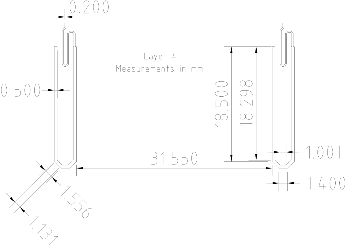 Figure 3-10 Layer 4 Marchand Balun
Dimensions
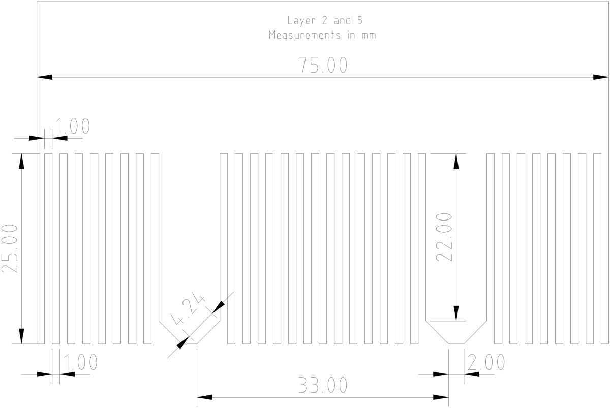 Figure 3-11 Layer 2 and 4 Ground Plane
Dimensions
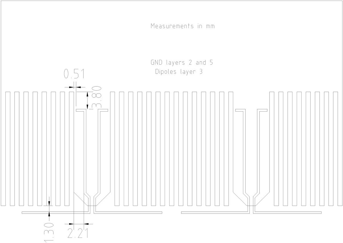 Figure 3-12 Dipole With Ground Plane
Dimensions
Figure 3-12 Dipole With Ground Plane
Dimensions| Layer Name | Type | Material | Thickness (mm) | Dielectric Material | Dielectric Constant |
|---|---|---|---|---|---|
| Top Solder | Solder Mask/Coverlay | Surface Material | 0.01016 | Solder Resist | 3.5 |
| Top Layer | Signal | Copper | 0.035 | ||
| Dielectric 1 | Dielectric | Core | 0.1 | FR-4 | 4.1 |
| Layer 2 | Signal | Copper | 0.01801 | ||
| Dielectric 2 | Dielectric | Prepreg | 0.2 | FR-4 | 4.1 |
| Layer 3 | Signal | Copper | 0.01901 | ||
| Dielectric 3 | Dielectric | Core | 0.1 | FR-4 | 4.1 |
| Layer 4 | Signal | Copper | 0.01801 | ||
| Dielectric 4 | Dielectric | Prepreg | 0.2 | FR-4 | 4.1 |
| Layer 5 | Signal | Copper | 0.01801 | ||
| Dielectric 5 | Dielectric | Core | 0.1 | FR-4 | 4.1 |
| Bottom Layer | Signal | Copper | 0.035 | ||
| Bottom Solder | Solder Mask/Coverlay | Surface Material | 0.01016 | Solder Resist | 3.5 |
See the TIDA-01632 Automotive Bluetooth® Low Energy car access satellite node reference design for more information on the design and for access to Gerber files, schematics, and more.