TIDA029A july 2019 – june 2023 CC2640R2F-Q1 , CC2642R , CC2642R-Q1
- 1
- Bluetooth Angle of Arrival (AoA) Antenna Design
- Trademarks
- 1Introduction
- 2Angle of Arrival Antenna Design Considerations
- 3Dipole Antenna Array
- 4Calculating AoA From IQ Measurements
- 5References
- 6Revision History
4.2.1 Bare PCB AoA With Compensation
The bare PCB required the least amount of compensation as the results were fairly close to Phi. However, Table 4-1 shows the gain and offset values used for each frequency.
Table 4-1 Bare PCB AoA Compensation
Values
| Frequency (MHz) | Channel | Gain | Offset |
|---|---|---|---|
| 2402 | 37 | 1.12 | –4.69 |
| 2404 | 0 | 1.12 | –4.69 |
| 2406 | 1 | 1.12 | –5.04 |
| 2408 | 2 | 1.14 | –4.82 |
| 2410 | 3 | 1.14 | –4.82 |
| 2412 | 4 | 1.14 | –5.1 |
| 2414 | 5 | 1.15 | –4.81 |
| 2416 | 6 | 1.15 | –4.73 |
| 2418 | 7 | 1.15 | –4.45 |
| 2420 | 8 | 1.15 | –4.73 |
| 2422 | 9 | 1.15 | –4.16 |
| 2424 | 10 | 1.15 | –4.37 |
| 2426 | 38 | 1.15 | –4.22 |
| 2428 | 11 | 1.15 | –4.36 |
| 2430 | 12 | 1.15 | –3.86 |
| 2432 | 13 | 1.14 | –3.65 |
| 2434 | 14 | 1.14 | –3.72 |
| 2436 | 15 | 1.15 | –3.57 |
| 2438 | 16 | 1.14 | –3.43 |
| 2440 | 17 | 1.14 | –3.29 |
| 2442 | 18 | 1.14 | –2.93 |
| 2444 | 19 | 1.12 | –3 |
| 2446 | 20 | 1.12 | –2.09 |
| 2448 | 21 | 1.12 | –2.79 |
| 2450 | 22 | 1.12 | –2.65 |
| 2452 | 23 | 1.12 | –2.57 |
| 2454 | 24 | 1.12 | –2.64 |
| 2456 | 25 | 1.12 | –2.36 |
| 2458 | 26 | 1.12 | –2.64 |
| 2460 | 27 | 1.12 | –2.36 |
| 2462 | 28 | 1.12 | –2.08 |
| 2464 | 29 | 1.11 | –2.49 |
| 2466 | 30 | 1.11 | –2.35 |
| 2468 | 31 | 1.11 | –2.63 |
| 2470 | 32 | 1.11 | –2.14 |
| 2472 | 33 | 1.11 | –2.55 |
| 2474 | 34 | 1.11 | –2.41 |
| 2476 | 35 | 1.11 | –2.07 |
| 2478 | 36 | 1.11 | –1.86 |
| 2480 | 39 | 1.09 | –1.99 |
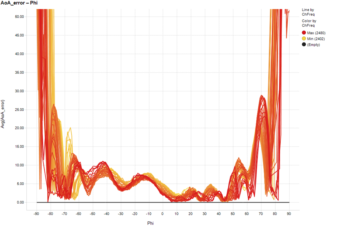
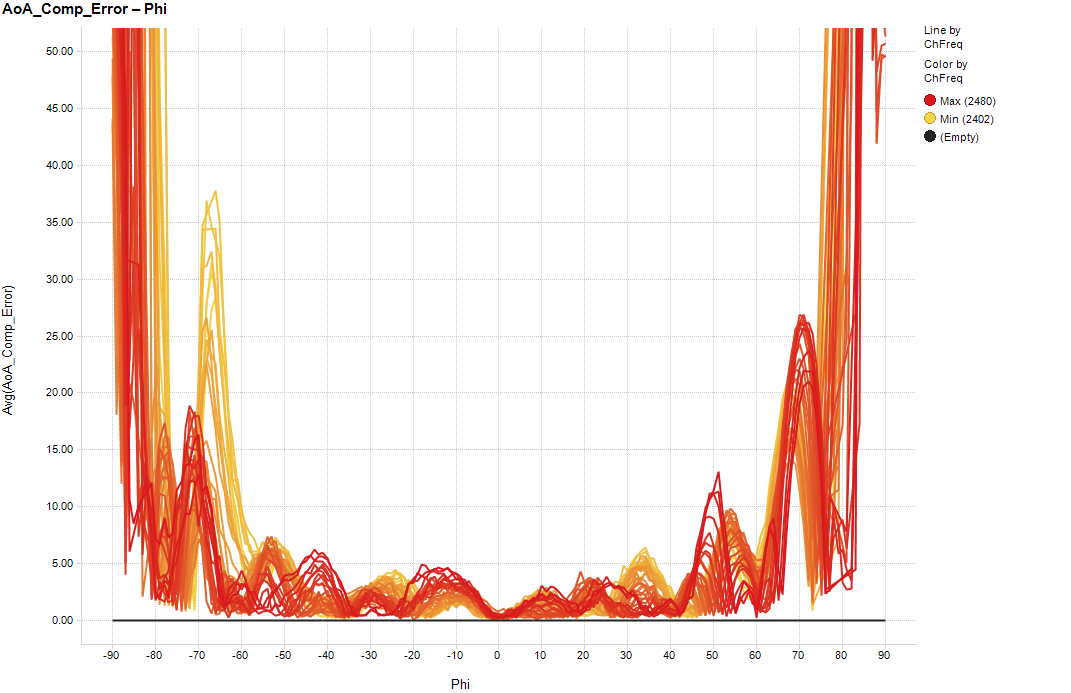
Figure 4-14 shows the uncompensated AoA error vs Phi (the actual angle) and Figure 4-15 the compensated AoA error vs Phi.
 Figure 4-14 Bare PCB Uncompensated AoA
Error Results
 Figure 4-15 Bare PCB Compensated AoA
Error Results
Figure 4-15 Bare PCB Compensated AoA
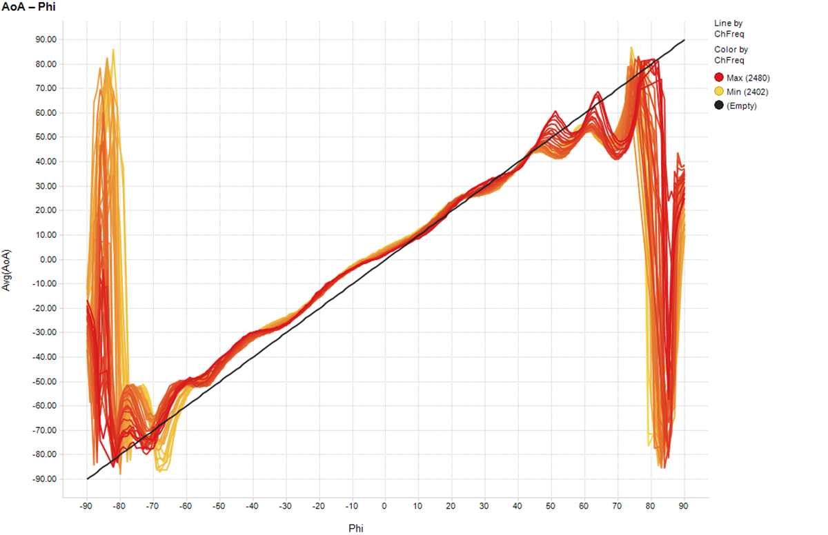
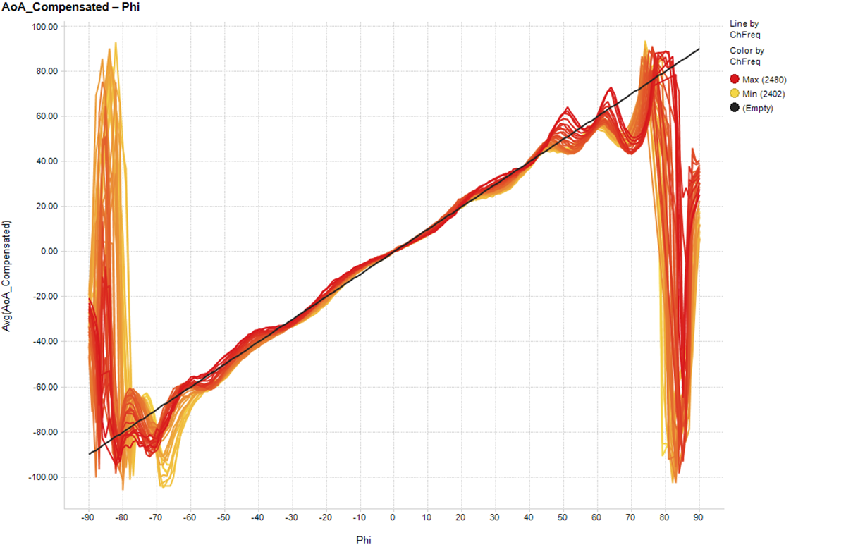
Error ResultsIt is clear that the error is greatly reduced over the most linear range (–65° to 65°). Figure 4-16 and Figure 4-17 show how the results have been adjusted to follow the ideal AoA vs Phi plot. There is less than 10° of error across the majority of frequencies from –70° to 65°.
 Figure 4-16 Bare PCB Uncompensated AoA
Results Over all Bluetooth Low Energy Channels
 Figure 4-17 Bare PCB Compensated AoA
Results Over all Bluetooth Low Energy Channels