TIDA029A july 2019 – june 2023 CC2640R2F-Q1 , CC2642R , CC2642R-Q1
- 1
- Bluetooth Angle of Arrival (AoA) Antenna Design
- Trademarks
- 1Introduction
- 2Angle of Arrival Antenna Design Considerations
- 3Dipole Antenna Array
- 4Calculating AoA From IQ Measurements
- 5References
- 6Revision History
3.4.2.3 PCB + RF Absorbing Material + Tin-Plated Copper Foil
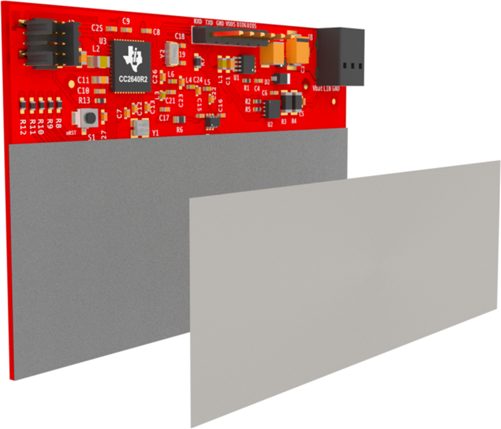
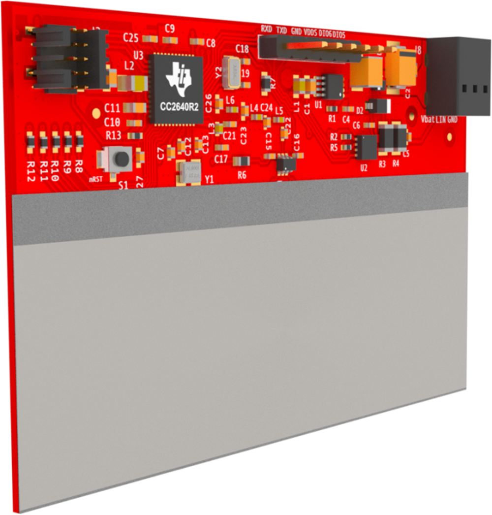
In this setup, one layer of WaveX WX-A-010-12P RF absorbing material from ARC Technologies and one layer of 3M® 1183 tin-plated copper foil is attached on the TIDA-01632 boards (opposite side from the incoming RF signal) shown in Figure 3-40 and Figure 3-41.
 Figure 3-40 PCB + RF Absorbing Material + Tin-Plated Copper Foil Detached
 Figure 3-41 PCB + RF Absorbing Material + Tin-Plated Copper Foil Attached
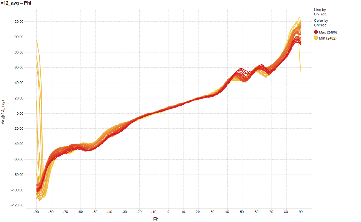
 Figure 3-42 PCB + RF Absorbing Material + Tin-Plated Copper Foil Phase Difference Over Angle Results
The tin-platted copper greatly improves the results from the hardware setup with only the RF absorbing material. Also, the wider angle phase difference error is reduced compared to the bare PCB as well showing a range of –75° to 75° with some error.