TIDA029A july 2019 – june 2023 CC2640R2F-Q1 , CC2642R , CC2642R-Q1
- 1
- Bluetooth Angle of Arrival (AoA) Antenna Design
- Trademarks
- 1Introduction
- 2Angle of Arrival Antenna Design Considerations
- 3Dipole Antenna Array
- 4Calculating AoA From IQ Measurements
- 5References
- 6Revision History
4.1 Dipole Antenna Array Uncompensated Angle of Arrival Results
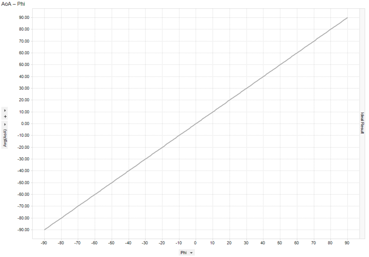
Using Equation 4, the angle of arrivals were calculated and plotted. Similar to the graphs in Section 3.4.2, the x-axis, Phi, is the actual angle the PCB was facing the transmitter and the y-axis is the average of the multiple calculated angle of arrivals from the multiple phase measurements. In addition, the lower the frequency the more yellow the trace and the higher the frequency the more red. The desired result shows the calculated AoA equal to Phi and the graphs display a perfect line showing that Phi equals AoA for all frequencies. This line is referenced on all AoA vs Phi graphs.
 Figure 4-3 Ideal AoA Result
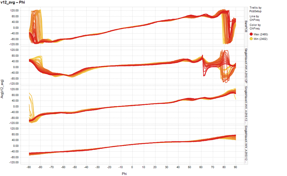
Figure 4-4 shows the results of all four different setups, with the bare PCB at the top, PCB + RF absorbing material second, PCB + RF absorbing material + tin-plated copper foil third, and PCB + RF absorbing material + tin-plated copper foil + metal at the bottom.
 Figure 4-4 All Hardware AoA Results Over all Bluetooth Low Energy Channels
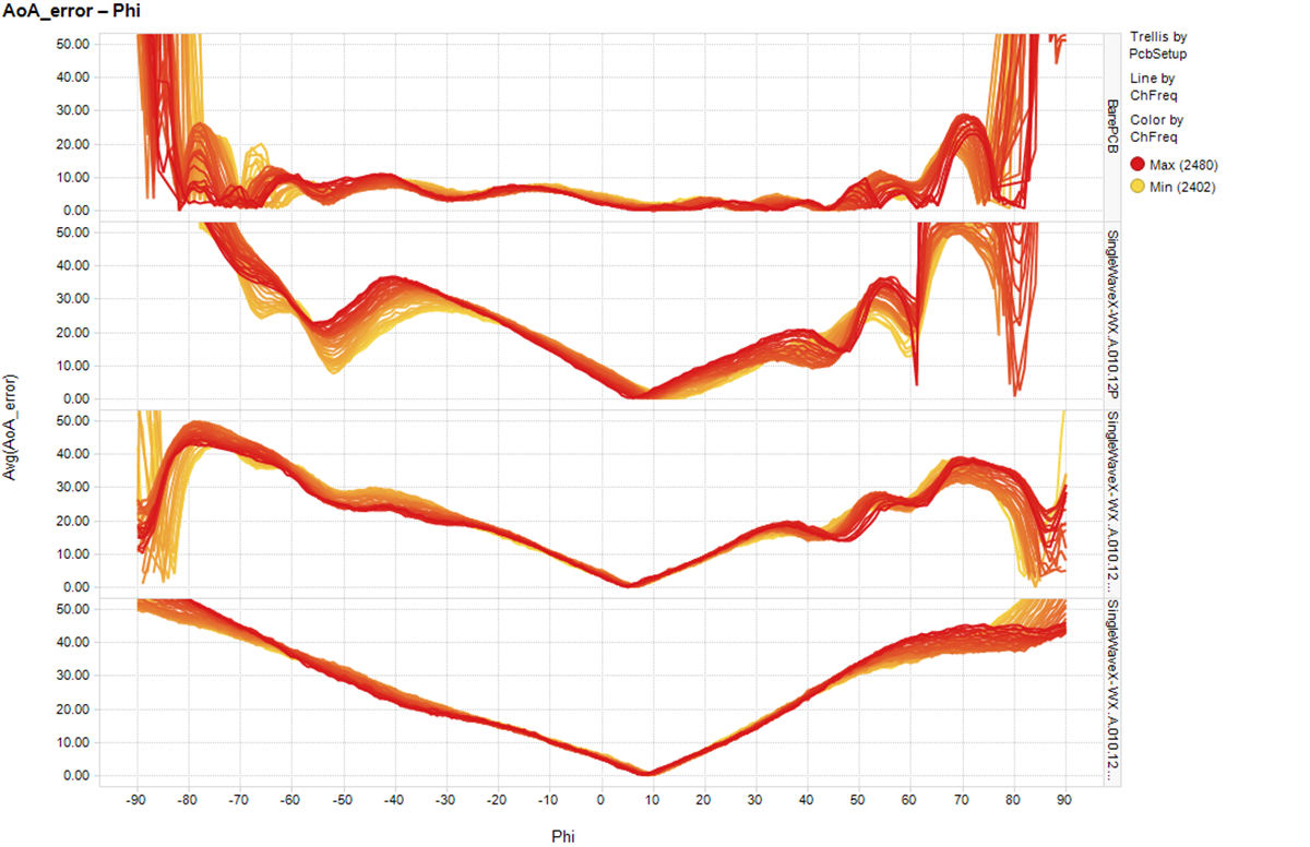
The bare PCB is the closest to measuring the true AoA but has large error as the angles get closer to ±90°. However, the PCB + RF absorbing material + tin-plated copper foil + metal setup has the most linear results at the widest angles. Figure 4-5 shows the error from the calculated AoA and the actual angle Phi.
 Figure 4-5 All Hardware AoA Error Results Over all Bluetooth Low Energy Channels
When interpreting the data, it is good to see consistent error as this can be compensated for as shown in Section 4.2. Notice that the PCB + RF absorbing material + tin-plated copper foil + metal has the most consistent error but needs compensation to improve the overall performance. With no compensation, the bare PCB shows the least error and most accurate results. The following subsections focus on the uncompensated AoA results for each test setup vs the actual AoA.