TIDA029A july   2019  – june 2023 CC2640R2F-Q1 , CC2642R , CC2642R-Q1


  1.   1
  2.   Bluetooth Angle of Arrival (AoA) Antenna Design
  3.   Trademarks
  4. 1Introduction
  5. 2Angle of Arrival Antenna Design Considerations
    1. 2.1 Antenna Spacing
    2. 2.2 RF Switch Considerations
  6. 3Dipole Antenna Array
    1. 3.1 Dipole Antenna Strengths and Weaknesses
    2. 3.2 Angle Measurement Plane
    3. 3.3 PCB Implementation
    4. 3.4 Two Dipole Array Test Results
      1. 3.4.1 Total Radiated Power (TRP)
      2. 3.4.2 Measuring Antenna 1 and 2 Phase Difference
        1. 3.4.2.1 Bare PCB
        2. 3.4.2.2 PCB + RF Absorbing Material
        3. 3.4.2.3 PCB + RF Absorbing Material + Tin-Plated Copper Foil
        4. 3.4.2.4 PCB + RF Absorbing Material + Tin-Plated Copper Foil + Metal
      3. 3.4.3 Phase Difference vs Distance
  7. 4Calculating AoA From IQ Measurements
    1. 4.1 Dipole Antenna Array Uncompensated Angle of Arrival Results
      1. 4.1.1 Bare PCB Uncompensated AoA
      2. 4.1.2 PCB + RF Absorbing Material Uncompensated AoA
      3. 4.1.3 PCB + RF Absorbing Material + Tin-Plated Copper Foil Uncompensated AoA
      4. 4.1.4 PCB + RF Absorbing Material + Tin-Plated Copper Foil + Metal Uncompensated AoA
    2. 4.2 Dipole Antenna Array Compensated AoA Results
      1. 4.2.1 Bare PCB AoA With Compensation
      2. 4.2.2 PCB + RF Absorbing Material + Tin-Plated Copper Foil Compensated AoA
      3. 4.2.3 PCB + RF Absorbing Material + Tin-Plated Copper Foil + Metal Compensated AoA
      4. 4.2.4 Hardware Setup Compensated Results Comparison
  8. 5References
  9. 6Revision History

PCB + RF Absorbing Material

In this setup, one layer of WaveX WX-A-010-12P RF absorbing material from ARC Technologies is attached on the TIDA-01632 board (on the opposite side from the incoming RF signal) shown in Figure 3-37 and Figure 3-38.
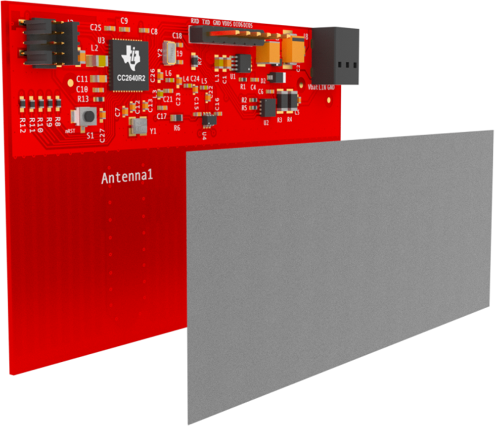
GUID-C70B0C84-E8AA-4CEB-8E6F-96EB7997CBF2-low.pngFigure 3-37 PCB + RF Absorbing Material Detached
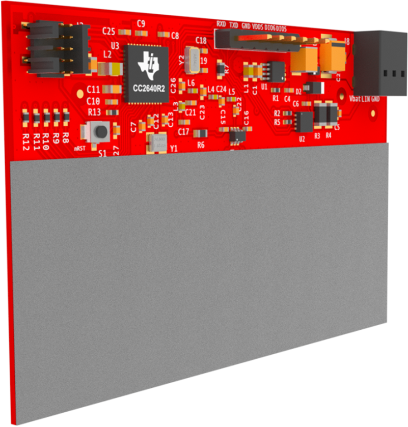
GUID-D45A3DBD-DE68-495F-8788-5FD9C2904CCD-low.pngFigure 3-38 PCB + RF Absorbing Material Attached
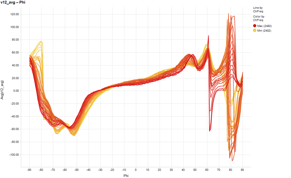
GUID-8BFC28D1-C0C4-43C4-8A73-BADD39C30C0D-low.pngFigure 3-39 PCB + RF Absorbing Material Phase Difference Over Angle Results

The RF absorbing material alone does not improve the measurements and is not recommended for final implementation.