TIDA029A july 2019 – june 2023 CC2640R2F-Q1 , CC2642R , CC2642R-Q1
- 1
- Bluetooth Angle of Arrival (AoA) Antenna Design
- Trademarks
- 1Introduction
- 2Angle of Arrival Antenna Design Considerations
- 3Dipole Antenna Array
- 4Calculating AoA From IQ Measurements
- 5References
- 6Revision History
4.2.4 Hardware Setup Compensated Results Comparison
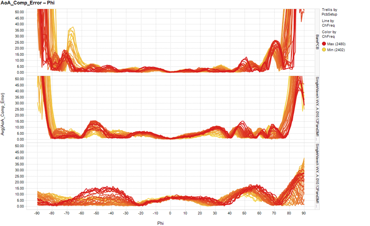
After implementing some basic linear compensation to the three hardware setups with the most linear IQ difference and AoA results, the compensated AoA results can be compared. Figure 4-26 shows all compensated AoA error vs Phi (the actual angle) with the bare PCB at the top, PCB + RF absorbing material + tin-plated copper foil in the middle, and PCB + RF absorbing material + tin-plated copper foil + metal at the bottom.
 Figure 4-26 Hardware Setup Comparison: Compensated AoA Error vs Phi
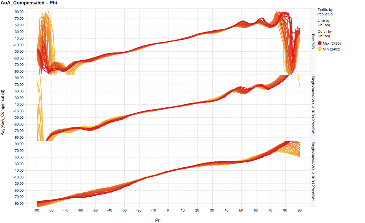
The comparison shows that the bare PCB shows the best results from approximately –65° to 65° but is the least accurate outside of that range. Adding the RF absorbing material and tin-plated copper foil reduces the error at the wider angles but at the cost of increased error from –30° to 35°. Adding the metal further decreases the error at the widest angles but also further increased the error from –20° to 20° and 40° to 70°. Again, better compensation could potentially improve the results for all hardware setups. Figure 4-27 shows the comparison of the three hardware setups compensated AoA over Phi in the same order as Figure 4-26.
 Figure 4-27 Hardware Setup Comparison: Compensated AoA Results
Figure 4-27 shows that for the full ±90° range, the PCB + RF absorbing material + tin-platted copper foil + metal provides the most stable results across all frequencies. All hardware setups become less linear as the angle gets wider, whether positive or negative. In addition, different frequencies provide more accurate results for specific angle ranges. It is important to remember that the antenna efficiency degrades when metal is close by. However, the data shows that the AoA range increases with the metal stand and tin-platted copper foil.
The tests results demonstrate the importance of testing and understanding the performance of the hardware setup. It is recommended to understand the behavior of the IQ difference measurements for a specific hardware setup to improve the AoA calculation and therefore the overall solutions AoA accuracy.