SBASB89 May   2025 ADS117L14 , ADS117L18

PRODUCTION DATA  

  1.   1
  2. Features
  3. Applications
  4. Description
  5. Pin Configuration and Functions
  6. Specifications
    1. 5.1 Absolute Maximum Ratings
    2. 5.2 ESD Ratings
    3. 5.3 Recommended Operating Conditions
    4. 5.4 Thermal Information
    5. 5.5 Electrical Characteristics
    6. 5.6 Timing Requirements
    7. 5.7 Switching Characteristics
    8. 5.8 Timing Diagrams
    9. 5.9 Typical Characteristics
  7. Parameter Measurement Information
    1. 6.1  Offset Error Measurement
    2. 6.2  Offset Drift Measurement
    3. 6.3  Gain Error Measurement
    4. 6.4  Gain Drift Measurement
    5. 6.5  NMRR Measurement
    6. 6.6  CMRR Measurement
    7. 6.7  PSRR Measurement
    8. 6.8  SNR Measurement
    9. 6.9  INL Error Measurement
    10. 6.10 THD Measurement
    11. 6.11 IMD Measurement
    12. 6.12 SFDR Measurement
    13. 6.13 Noise Performance
  8. Detailed Description
    1. 7.1 Overview
    2. 7.2 Functional Block Diagram
    3. 7.3 Feature Description
      1. 7.3.1 Analog Inputs (AINP, AINN)
        1. 7.3.1.1 Input Range
      2. 7.3.2 Reference Voltage (REFP, REFN)
        1. 7.3.2.1 Reference Voltage Range
      3. 7.3.3 Clock Operation
        1. 7.3.3.1 Clock Dividers
        2. 7.3.3.2 Internal Oscillator
        3. 7.3.3.3 External Clock
      4. 7.3.4 Power-On Reset (POR)
      5. 7.3.5 VCM Output Voltage
      6. 7.3.6 GPIO
      7. 7.3.7 Modulator
      8. 7.3.8 Digital Filter
        1. 7.3.8.1 Wideband Filter
        2. 7.3.8.2 Low-Latency Filter (Sinc)
          1. 7.3.8.2.1 Sinc4 Filter
          2. 7.3.8.2.2 Sinc4 + Sinc1 Cascade Filter
          3. 7.3.8.2.3 Sinc3 Filter
          4. 7.3.8.2.4 Sinc3 + Sinc1 Filter
    4. 7.4 Device Functional Modes
      1. 7.4.1 Reset
        1. 7.4.1.1 RESET Pin
        2. 7.4.1.2 Reset by SPI Register
        3. 7.4.1.3 Reset by SPI Input Pattern
      2. 7.4.2 Idle and Standby Modes
      3. 7.4.3 Power-Down
      4. 7.4.4 Speed Modes
      5. 7.4.5 Synchronization
        1. 7.4.5.1 Synchronized Control Mode
        2. 7.4.5.2 Start/Stop Control Mode
      6. 7.4.6 Conversion-Start Delay Time
      7. 7.4.7 Calibration
        1. 7.4.7.1 Offset Calibration Registers
        2. 7.4.7.2 Gain Calibration Registers
        3. 7.4.7.3 Calibration Procedure
      8. 7.4.8 Diagnostics
        1. 7.4.8.1 ERROR Pin and ERR_FLAG Bit
        2. 7.4.8.2 SPI CRC
        3. 7.4.8.3 Register Map CRC
        4. 7.4.8.4 ADC Error
        5. 7.4.8.5 SPI Address Range
        6. 7.4.8.6 SCLK Counter
        7. 7.4.8.7 Clock Counter
        8. 7.4.8.8 Frame-Sync CRC
        9. 7.4.8.9 Self Test
      9. 7.4.9 Frame-Sync Data Port
        1. 7.4.9.1  Data Packet
        2. 7.4.9.2  Data Format
        3. 7.4.9.3  STATUS_DP Header Byte
        4. 7.4.9.4  FSYNC Pin
        5. 7.4.9.5  DCLK Pin
        6. 7.4.9.6  DOUTx Pins
        7. 7.4.9.7  DINx Pins
        8. 7.4.9.8  Time Division Multiplexing
        9. 7.4.9.9  Daisy Chain
        10. 7.4.9.10 DOUTx Timing
    5. 7.5 Programming
      1. 7.5.1 Hardware Programming
      2. 7.5.2 SPI Programming
        1. 7.5.2.1 Chip Select (CS)
        2. 7.5.2.2 Serial Clock (SCLK)
        3. 7.5.2.3 Serial Data Input (SDI)
        4. 7.5.2.4 Serial Data Output (SDO)
      3. 7.5.3 SPI Frame
      4. 7.5.4 Commands
        1. 7.5.4.1 Write Register Command
        2. 7.5.4.2 Read Register Command
      5. 7.5.5 SPI Daisy-Chain
  9. Register Map
  10. Application and Implementation
    1. 9.1 Application Information
      1. 9.1.1 Input Driver
      2. 9.1.2 Anti-alias Filter
      3. 9.1.3 Reference Voltage
    2. 9.2 Typical Application
      1. 9.2.1 Design Requirements
      2. 9.2.2 Detailed Design Procedure
      3. 9.2.3 Application Curves
    3. 9.3 Power Supply Recommendations
      1. 9.3.1 AVDD1 and AVSS
      2. 9.3.2 AVDD2
      3. 9.3.3 IOVDD
      4. 9.3.4 CAPA and CAPD
    4. 9.4 Layout
      1. 9.4.1 Layout Guidelines
      2. 9.4.2 Layout Example
  11. 10Device and Documentation Support
    1. 10.1 Documentation Support
      1. 10.1.1 Related Documentation
    2. 10.2 Receiving Notification of Documentation Updates
    3. 10.3 Support Resources
    4. 10.4 Trademarks
    5. 10.5 Electrostatic Discharge Caution
    6. 10.6 Glossary
  12. 11Revision History
  13. 12Mechanical, Packaging, and Orderable Information

Package Options

Mechanical Data (Package|Pins)
Thermal pad, mechanical data (Package|Pins)
Orderable Information
Sinc3 + Sinc1 Filter

The sinc3 + sinc1 filter mode is the cascade of the sinc3 and a sinc1 filter. The OSR of the sinc3 stage is fixed (OSR = 32000) and the OSR of the sinc1 stage is programmable to 3 and 5. Table 7-6 summarizes the characteristics of the sinc3 + sinc1 filter.

Table 7-6 Sinc3 + Sinc1 Filter Characteristics
MODEfCLK
(MHz)
OSR
(A × B) (1)
DATA RATE (SPS)–3dB FREQUENCY
(Hz)
LATENCY
(ms)
NMRR AT FIRST NULL (dB)
2% CLOCK TOLERANCE6% CLOCK TOLERANCE
Max speed32.76896000
(32000 × 3)
170699.773426
High speed25.6133.35412.5
Mid speed12.866.62725
Low speed3.216.76.7100
Max speed32.768160000
(32000 × 5)
10243.513.73426
High speed25.6803417.5
Mid speed12.8401735
Low speed3.2104.2140
A = First stage OSR, B = Second stage OSR.

Figure 7-23 shows the frequency response of the sinc3 + sinc1 filter. The frequency response exhibits the characteristic sinc filter response lobes and nulls. The nulls occur at fDATA and at multiples thereof. Figure 7-24 shows the detailed response in the region of 0.9 to 1.1 · fIN / fDATA.
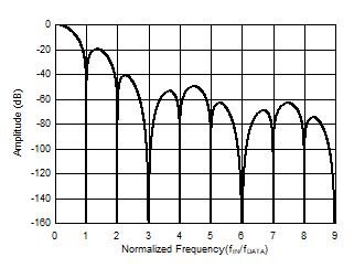
ADS117L14 ADS117L18 Sinc3 + Sinc1 Frequency
                        ResponseFigure 7-23 Sinc3 + Sinc1 Frequency Response
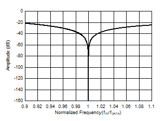
ADS117L14 ADS117L18 Detail Sinc3 + Sinc1
                        Frequency ResponseFigure 7-24 Detail Sinc3 + Sinc1 Frequency Response