SLUA963B June 2020 – October 2022 UCC21710-Q1 , UCC21732-Q1 , UCC5870-Q1
- HEV/EV Traction Inverter Design Guide Using Isolated IGBT and SiC Gate Drivers
- 1Introduction
- 2HEV/EV Overview
-
3Design of HEV/EV Traction Inverter Drive Stage
- 3.1 Introduction to UCC217xx-Q1
- 3.2 Designing a Traction Inverter Drive System Using UCC217xx-Q1
- 3.3 Description of Protection Features
- 3.4 Protection Features of UCC217xx-Q1
- 3.5
UCC217xx-Q1 Protection and Monitoring Features Descriptions
- 3.5.1 Primary and Secondary Side UVLO and OVLO
- 3.5.2 Over-Current (OC) and Desaturation (DESAT) Detection
- 3.5.3 2-Level and Soft Turn-Off
- 3.5.4 Power Switch Gate Voltage (VGE/VGS) Monitoring
- 3.5.5 Power Switch Anti-Shoot-Through
- 3.5.6 Integrated Internal or External Miller Clamp
- 3.5.7 Isolated Analog-to-PWM Channel
- 3.5.8 Short-Circuit Clamping
- 3.5.9 Active Pulldown
- 3.6 Introduction to UCC5870-Q1
- 3.7 Designing a Traction Inverter Drive System Using UCC5870-Q1
- 3.8 Description of Protection Features
- 3.9 Protection Features of UCC5870-Q1
- 3.10
UCC5870-Q1 Protection and Monitoring Features Descriptions
- 3.10.1 Primary and Secondary Side UVLO and OVLO
- 3.10.2 Programmable Desaturation (DESAT) Detection and Over-Current (OC)
- 3.10.3 Adjustable 2-Level or Soft Turn-Off
- 3.10.4 Active High-Voltage Clamp
- 3.10.5 Power Switch Gate Voltage (VGE/VGS) Monitoring
- 3.10.6 Gate Threshold Voltage Monitor
- 3.10.7 Power Switch Anti-Shoot-Through
- 3.10.8 Active Short Circuit (ASC)
- 3.10.9 Integrated Internal or External Miller Clamp
- 3.10.10 Isolated Analog-to-Digital Converter
- 3.10.11 Short-Circuit Clamping
- 3.10.12 Active and Passive Pulldown
- 3.10.13 Thermal Shutdown and Temperature Warning of Driver IC
- 3.10.14 Clock Monitor and CRC
- 3.10.15 SPI and Register Data Protection
- 4Isolated Bias Supply Architecture
- 5Summary
- 6References
- 7Revision History
3.10.8 Active Short Circuit (ASC)
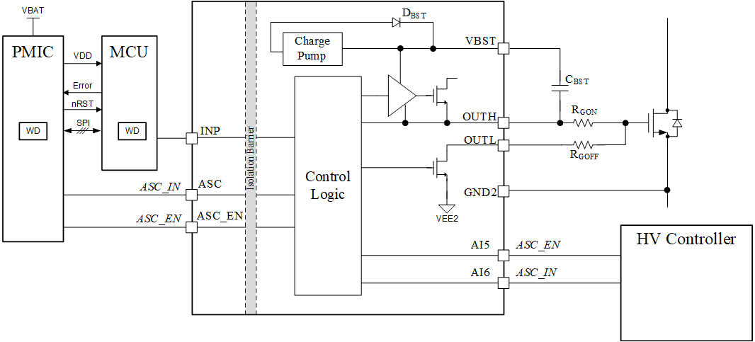
The active short circuit (ASC) function allows the system to force the state of the power transistor regardless of the PWM input. The ASC interface is located on both the primary and secondary sides, depending on the architecture of the safety controller. For cases where the main MCU is not available due to fault or otherwise, a secondary control circuit drives the ASC_EN input high to force the output of the UCC5870-Q1 to the state defined by the ASC input, denoted as the HV Controller in Figure 3-24.
From system point of view, the implementation of ASC function is to control the inverter output to be a zero vector. The zero vector can be generated through two approaches: Main MCU or secondary control circuit. The ASC function is usually triggered when there is a system fault. If the fault is not a MCU fault, the MCU can implement diagnosis through the SPI interface and generate the appropriate zero vector based on fault type. If the fault happens in the MCU, then the secondary control circuit pulls the ASC_EN pin to be HIGH and suitable state on the ASC pin. With the ASC_EN pin pulled high, the driver output follows the state on the ASC pin. For the primary side, two dedicated inputs are available for the ASC control. The ASC control is also available on the secondary side using the AI5 and AI6 inputs. The driver is configured with the secondary ASC function using SPI. In this configuration, AI5 works as ASC_EN and AI6 is the ASC input. The primary and secondary ASC interfaces are shown in Figure 3-24.
 Figure 3-24 ASC primary and secondary side interfaces