SLUA963B June 2020 – October 2022 UCC21710-Q1 , UCC21732-Q1 , UCC5870-Q1
- HEV/EV Traction Inverter Design Guide Using Isolated IGBT and SiC Gate Drivers
- 1Introduction
- 2HEV/EV Overview
-
3Design of HEV/EV Traction Inverter Drive Stage
- 3.1 Introduction to UCC217xx-Q1
- 3.2 Designing a Traction Inverter Drive System Using UCC217xx-Q1
- 3.3 Description of Protection Features
- 3.4 Protection Features of UCC217xx-Q1
- 3.5
UCC217xx-Q1 Protection and Monitoring Features Descriptions
- 3.5.1 Primary and Secondary Side UVLO and OVLO
- 3.5.2 Over-Current (OC) and Desaturation (DESAT) Detection
- 3.5.3 2-Level and Soft Turn-Off
- 3.5.4 Power Switch Gate Voltage (VGE/VGS) Monitoring
- 3.5.5 Power Switch Anti-Shoot-Through
- 3.5.6 Integrated Internal or External Miller Clamp
- 3.5.7 Isolated Analog-to-PWM Channel
- 3.5.8 Short-Circuit Clamping
- 3.5.9 Active Pulldown
- 3.6 Introduction to UCC5870-Q1
- 3.7 Designing a Traction Inverter Drive System Using UCC5870-Q1
- 3.8 Description of Protection Features
- 3.9 Protection Features of UCC5870-Q1
- 3.10
UCC5870-Q1 Protection and Monitoring Features Descriptions
- 3.10.1 Primary and Secondary Side UVLO and OVLO
- 3.10.2 Programmable Desaturation (DESAT) Detection and Over-Current (OC)
- 3.10.3 Adjustable 2-Level or Soft Turn-Off
- 3.10.4 Active High-Voltage Clamp
- 3.10.5 Power Switch Gate Voltage (VGE/VGS) Monitoring
- 3.10.6 Gate Threshold Voltage Monitor
- 3.10.7 Power Switch Anti-Shoot-Through
- 3.10.8 Active Short Circuit (ASC)
- 3.10.9 Integrated Internal or External Miller Clamp
- 3.10.10 Isolated Analog-to-Digital Converter
- 3.10.11 Short-Circuit Clamping
- 3.10.12 Active and Passive Pulldown
- 3.10.13 Thermal Shutdown and Temperature Warning of Driver IC
- 3.10.14 Clock Monitor and CRC
- 3.10.15 SPI and Register Data Protection
- 4Isolated Bias Supply Architecture
- 5Summary
- 6References
- 7Revision History
4 Isolated Bias Supply Architecture
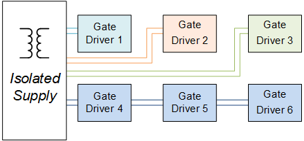
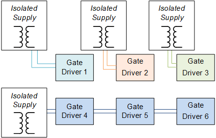
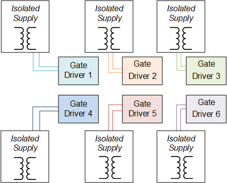
Another important consideration in automotive traction inverter systems with regards to the gate drivers is the bias supply architecture. The bias supplies are used to provide isolated power used to drive each IGBT or SiC MOSFET. The reliability of the single or multiple isolated supplies is necessary to keep the inverter operational. The architectures of the gate driver bias supplies varies based on the required level of reliability. The bias supplies may be shared amongst multiple drivers (centralized), provided separately to each driver (distributed), or partially shared (semi-distributed).
Centralized bias supply architecture has the advantage of low component count, low cost, and generic control. However, the transformer for this architecture may be bulky, can suffer from common mode current, can result in complex PCB routing when shared amongst six drivers and does not inherently contain any redundancy.
 Figure 4-1 Centralized Bias Supply Architecture
The semi-distributed power consists of several transformers to generate the biases for various groups of drivers. For example, each high-side driver may be supplied with a separate transformer whereas all the low-side drivers may be shared. The advantage of this architecture is the simplicity of transformer construction and PCB layout, the ability to have higher power quality for each bias supply, the distribution of weight of the supplies' transformers, and the simplicity of control. The disadvantages include higher component count, higher cost, and still a lack of redundancy.
 Figure 4-2 Semi-Distributed Bias Supply Architecture
Finally, the distributed power architecture provides a separate bias supply for each gate driver. Although it requires more components, resulting in higher cost, the advantages include a high level of redundancy, simplified layout and distribution of weight and better power quality.
 Figure 4-3 Distributed Bias Supply Architecture
For more information on bias supplies, please see TI's portfolio of high-voltage controllers and this reference design on bias supplies for HEV/EV traction inverters.