SLUA963B June 2020 – October 2022 UCC21710-Q1 , UCC21732-Q1 , UCC5870-Q1
- HEV/EV Traction Inverter Design Guide Using Isolated IGBT and SiC Gate Drivers
- 1Introduction
- 2HEV/EV Overview
-
3Design of HEV/EV Traction Inverter Drive Stage
- 3.1 Introduction to UCC217xx-Q1
- 3.2 Designing a Traction Inverter Drive System Using UCC217xx-Q1
- 3.3 Description of Protection Features
- 3.4 Protection Features of UCC217xx-Q1
- 3.5
UCC217xx-Q1 Protection and Monitoring Features Descriptions
- 3.5.1 Primary and Secondary Side UVLO and OVLO
- 3.5.2 Over-Current (OC) and Desaturation (DESAT) Detection
- 3.5.3 2-Level and Soft Turn-Off
- 3.5.4 Power Switch Gate Voltage (VGE/VGS) Monitoring
- 3.5.5 Power Switch Anti-Shoot-Through
- 3.5.6 Integrated Internal or External Miller Clamp
- 3.5.7 Isolated Analog-to-PWM Channel
- 3.5.8 Short-Circuit Clamping
- 3.5.9 Active Pulldown
- 3.6 Introduction to UCC5870-Q1
- 3.7 Designing a Traction Inverter Drive System Using UCC5870-Q1
- 3.8 Description of Protection Features
- 3.9 Protection Features of UCC5870-Q1
- 3.10
UCC5870-Q1 Protection and Monitoring Features Descriptions
- 3.10.1 Primary and Secondary Side UVLO and OVLO
- 3.10.2 Programmable Desaturation (DESAT) Detection and Over-Current (OC)
- 3.10.3 Adjustable 2-Level or Soft Turn-Off
- 3.10.4 Active High-Voltage Clamp
- 3.10.5 Power Switch Gate Voltage (VGE/VGS) Monitoring
- 3.10.6 Gate Threshold Voltage Monitor
- 3.10.7 Power Switch Anti-Shoot-Through
- 3.10.8 Active Short Circuit (ASC)
- 3.10.9 Integrated Internal or External Miller Clamp
- 3.10.10 Isolated Analog-to-Digital Converter
- 3.10.11 Short-Circuit Clamping
- 3.10.12 Active and Passive Pulldown
- 3.10.13 Thermal Shutdown and Temperature Warning of Driver IC
- 3.10.14 Clock Monitor and CRC
- 3.10.15 SPI and Register Data Protection
- 4Isolated Bias Supply Architecture
- 5Summary
- 6References
- 7Revision History
2.2 HEV/EV Traction Inverter System Architecture
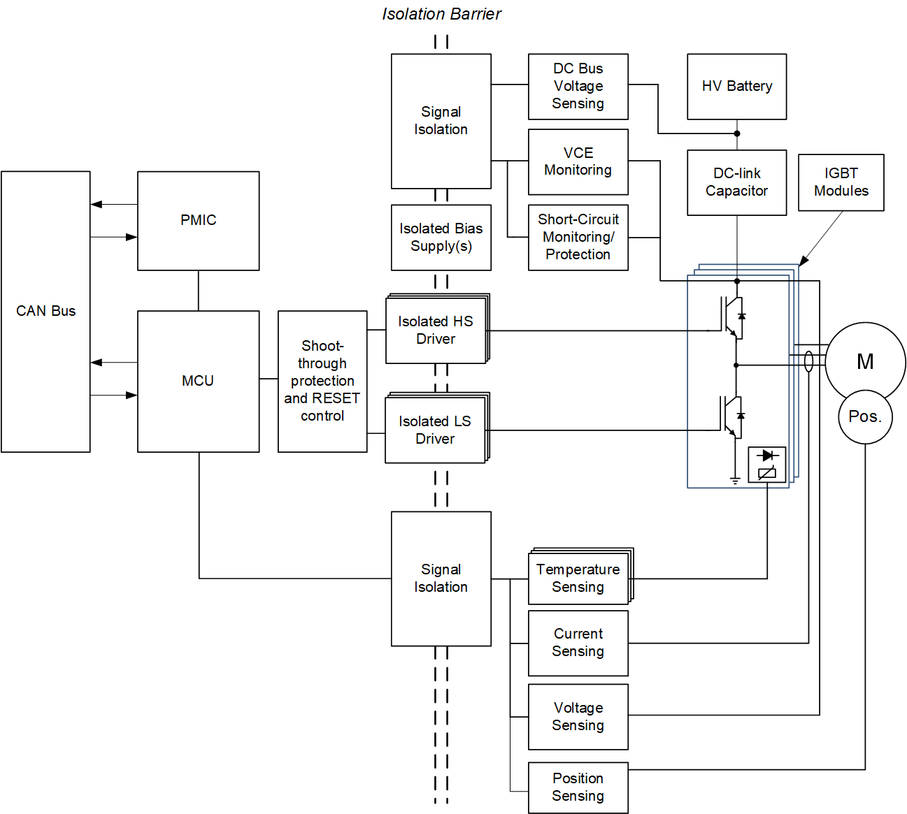
Zooming in to the traction inverter system reveals multiple blocks including the power management IC (PMIC) and the microcontroller (MCU), the high-power IGBT or SiC MOSFET power modules and their temperature sensing elements, the high-voltage (HV) battery, the DC-link capacitor, sensing blocks, various protection and monitoring circuits and signal isolation, shown in Figure 2-4. The high-power switches are the most critical component in the inverter as they control the flow of current to the motor to generate motion. As such, the switches' are monitored and protected by sensing their temperature, voltage and current throughout their operation. The switches are controlled via the MCU and isolated gate drivers for the high side (HS) and low side (LS) of the inverter leg. The PWM signals are commonly generated using the space vector modulation (SVM) scheme. As the motor operates, the voltage, current and position signals are sensed and fed back to the controller to modify the modulation of the inverter. One such feedback method is field oriented control (FOC), which uses two phases of current and the position to generate the proper vector of modulation. A good modulation scheme, fast feedback and accurately sensed signals are required for efficient motoring.
 Figure 2-4 High-Voltage Traction Inverter Block Diagram
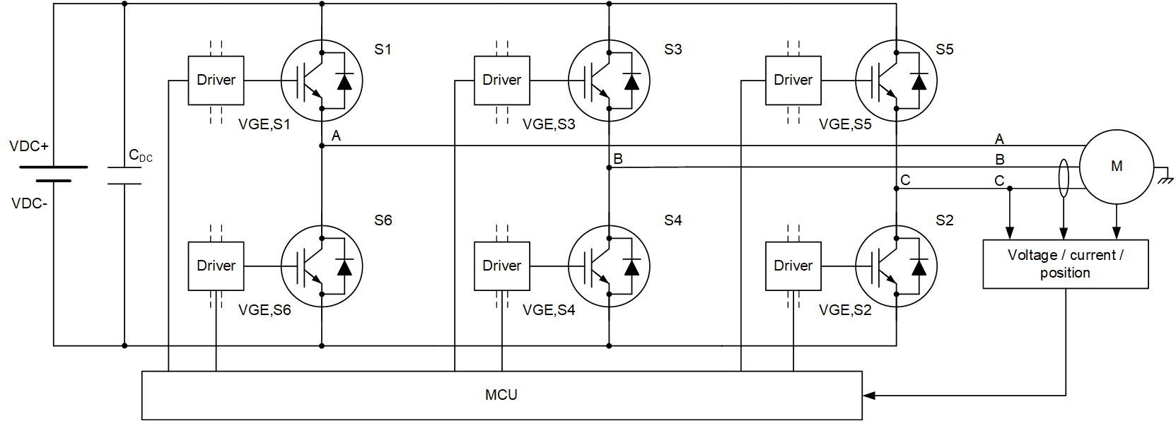
A closer look at the inverter, shown in Figure 2-5, reveals six total semiconductor power switching devices with a gate driver to amplify the PWM signal from the MCU. The three legs of the inverter convert the DC battery voltage into three phases of AC voltage and current to drive the motor. Two current measurements and a position measurement are fed back to the MCU for FOC which utilizes mathematical transformations to generate the proper signals for the six switches to control the output voltages at phases A, B and C.
 Figure 2-5 Three-Phase Two-Level Inverter Using IGBTs
In vector modulation, eight total states are available where two are zero vectors and the rest are active vectors used to apply the necessary voltage to the motor to generate the proper amount of torque. Table 2-1 shows the states where switch pairs S1 and S6, S3 and S4, and S5 and S2 are complementary to one another.
| Vector | S1 | S2 | S3 | S4 | S5 | S6 | VAB | VBC | VCA | Vector Mode |
|---|---|---|---|---|---|---|---|---|---|---|
| {000} | OFF | ON | OFF | ON | OFF | ON | 0 | 0 | 0 | Zero |
| {100} | ON | ON | OFF | ON | OFF | OFF | +VDC | 0 | -VDC | Active |
| {100} | ON | ON | ON | OFF | OFF | OFF | 0 | +VDC | -VDC | Active |
| {010} | OFF | ON | ON | OFF | OFF | ON | -VDC | +VDC | 0 | Active |
| {011} | OFF | OFF | ON | OFF | ON | ON | -VDC | 0 | +VDC | Active |
| {001} | OFF | OFF | OFF | ON | ON | ON | 0 | -VDC | +VDC | Active |
| {101} | ON | OFF | OFF | ON | ON | OFF | +VDC | -VDC | 0 | Active |
| {111} | ON | OFF | ON | OFF | ON | OFF | 0 | 0 | 0 | Zero |
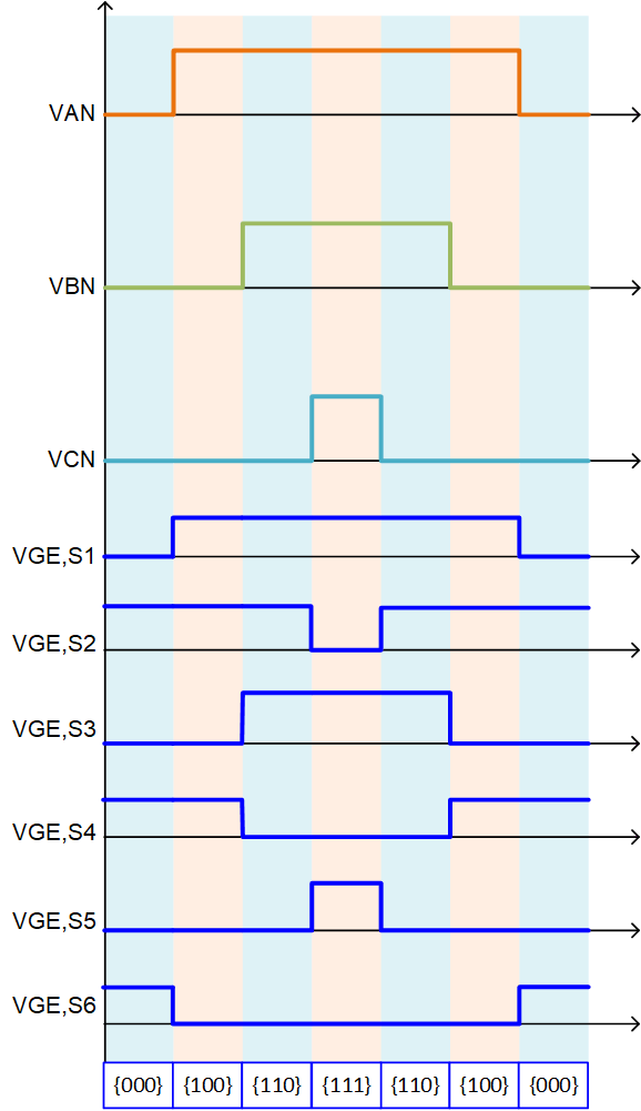
There are various methods of implementing SVM. Tradeoffs between the SVM methods include reduction of switching losses, bus voltage maximum utilization, reduced harmonic content, while still achieving precise control. One such method is seven segment SVM, which is beneficial to produce a voltage waveform with low harmonics, and thus less distortion when driving the motor. The gating sequence is shown in Figure 2-6. A single skipped or extra gate signal as a result of an MCU control error or gate driver latched output as a result of a failure could result in inverter output distortion. Overlap of complementary switches in a phase leg could result in shoot through, and must always be avoided. As shown, the commutation of the motor is dependent on very specific gating sequences. Thus, it would be very difficult to unintentionally commutate the motor with a one-off gate driver failure.
 Figure 2-6 Seven Segment SVM
Aside from an effective gating sequence as generated by the MCU, a smart drive system includes gate drivers with protection and monitoring capabilities to protect the power switch. The following sections discuss the traction inverter system impact due to various failures within the system and how the gate drive and surrounding circuits are used to enhance the reliability of the system.