SLUA963B June 2020 – October 2022 UCC21710-Q1 , UCC21732-Q1 , UCC5870-Q1
- HEV/EV Traction Inverter Design Guide Using Isolated IGBT and SiC Gate Drivers
- 1Introduction
- 2HEV/EV Overview
-
3Design of HEV/EV Traction Inverter Drive Stage
- 3.1 Introduction to UCC217xx-Q1
- 3.2 Designing a Traction Inverter Drive System Using UCC217xx-Q1
- 3.3 Description of Protection Features
- 3.4 Protection Features of UCC217xx-Q1
- 3.5
UCC217xx-Q1 Protection and Monitoring Features Descriptions
- 3.5.1 Primary and Secondary Side UVLO and OVLO
- 3.5.2 Over-Current (OC) and Desaturation (DESAT) Detection
- 3.5.3 2-Level and Soft Turn-Off
- 3.5.4 Power Switch Gate Voltage (VGE/VGS) Monitoring
- 3.5.5 Power Switch Anti-Shoot-Through
- 3.5.6 Integrated Internal or External Miller Clamp
- 3.5.7 Isolated Analog-to-PWM Channel
- 3.5.8 Short-Circuit Clamping
- 3.5.9 Active Pulldown
- 3.6 Introduction to UCC5870-Q1
- 3.7 Designing a Traction Inverter Drive System Using UCC5870-Q1
- 3.8 Description of Protection Features
- 3.9 Protection Features of UCC5870-Q1
- 3.10
UCC5870-Q1 Protection and Monitoring Features Descriptions
- 3.10.1 Primary and Secondary Side UVLO and OVLO
- 3.10.2 Programmable Desaturation (DESAT) Detection and Over-Current (OC)
- 3.10.3 Adjustable 2-Level or Soft Turn-Off
- 3.10.4 Active High-Voltage Clamp
- 3.10.5 Power Switch Gate Voltage (VGE/VGS) Monitoring
- 3.10.6 Gate Threshold Voltage Monitor
- 3.10.7 Power Switch Anti-Shoot-Through
- 3.10.8 Active Short Circuit (ASC)
- 3.10.9 Integrated Internal or External Miller Clamp
- 3.10.10 Isolated Analog-to-Digital Converter
- 3.10.11 Short-Circuit Clamping
- 3.10.12 Active and Passive Pulldown
- 3.10.13 Thermal Shutdown and Temperature Warning of Driver IC
- 3.10.14 Clock Monitor and CRC
- 3.10.15 SPI and Register Data Protection
- 4Isolated Bias Supply Architecture
- 5Summary
- 6References
- 7Revision History
3.5.2 Over-Current (OC) and Desaturation (DESAT) Detection
Overcurrent (OC) protection (UCC21732-Q1 and UCC21710-Q1) and desaturation (DESAT) protection (UCC21750-Q1) are used to prevent a short-circuit event from destroying the power devices. Both OC and DESAT protection are available with UCC217xx variants and are integrated internally, with a few external components based on the application. The OC and DESAT protection ST (self-test) circuits may be implemented externally and are shown below.
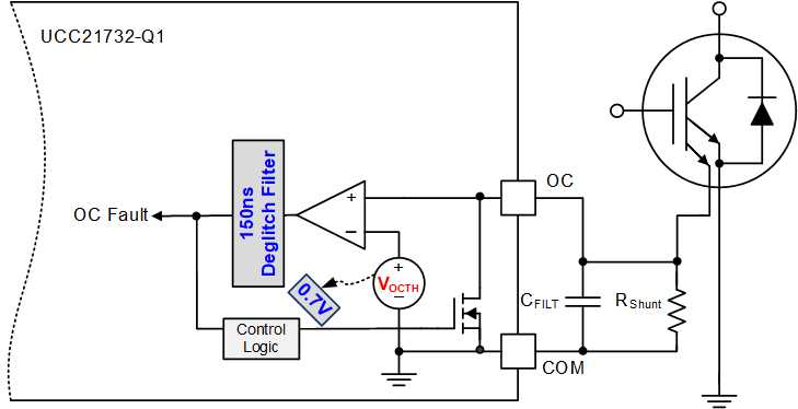
Integrated OC protection is shown in Figure 3-4. In this example, the IGBT's current is stepped down with an integrated current mirror and is output at the split emitter. The current is then measured via a shunt resistor, RShunt. The OC pin monitors the current via the voltage across RShunt and triggers the OC fault when the voltage surpasses the internal threshold of 0.7 V. At this time, the driver will initiate soft turn-off and/or 2-level turn-off to safely shut down the power device.
 Figure 3-4 Overcurrent and Short Circuit Protection (UCC21732-Q1 and UCC21710-Q1)
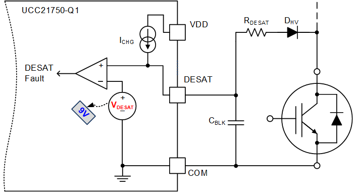
Desaturation detection, or DESAT is a method most commonly used with IGBTs because of their well-defined knee point in the I-V curve at which the device moves from the linear to the active region as a short circuit occurs. The DESAT pin utilizes this information by monitoring the voltage across the IGBT when it is turned on. The DESAT pin is connected to the collector of the IGBT through a series resistor and HV diode, DHV. DHV becomes forward biased when the voltage at the IGBT increases beyond the DESAT threshold voltage of 9 V. RDESAT limits the current flowing to the DESAT pin. The timing is controlled by CBLK, which charges up to the threshold voltage when the driver turns on. The DESAT threshold voltage can be adjusted manually with the addition of more DHV diodes in series or by adding a Zener diode in series.
 Figure 3-5 DESAT Protection (UCC21750)
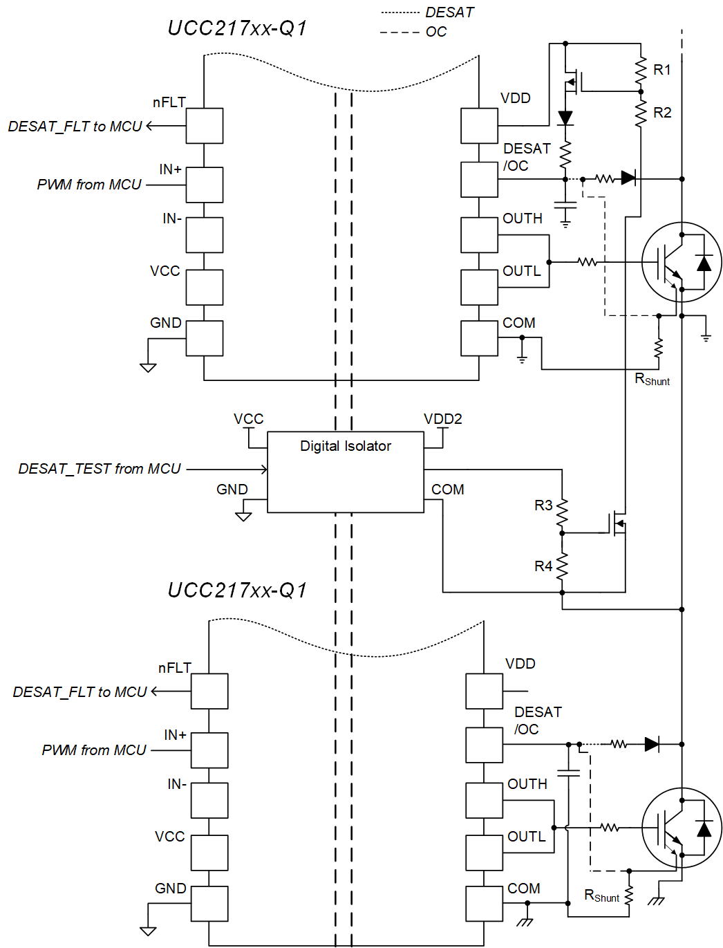
The self-test circuit for the OC or DESAT detection is performed via external circuitry controlled by the MCU through a digital isolator, shown in Figure 3-6. A digital isolator is used to drive the gate of a NMOS FET to enable a fault at the DESAT/OC pin. The NMOS FET is turned on and causes the upper PMOS FET to become turned on, which allows current sourced from VDD to increase the voltage at the pin to beyond the threshold voltage. At this point, the nFLT will trigger. The input, IN+, must be high during this self-test for nFLT to trigger. If nFLT is triggered, then the short circuit detection is working properly. For more information on this circuit design and implementation, please read SiC/IGBT Isolated Gate Driver Reference Design With Thermal Diode and Sensing FET.
 Figure 3-6 DESAT/OC Detection Self-Test Circuit