SLVA372D November 2009 – November 2022 LM2577 , LM2585 , LM2586 , LM2587 , LM2588 , LMR61428 , LMR62014 , LMR62421 , LMR64010 , TL1451A , TL5001 , TL5001A , TLV61220 , TPS40210 , TPS40211 , TPS43000 , TPS61000 , TPS61002 , TPS61005 , TPS61006 , TPS61007 , TPS61010 , TPS61012 , TPS61013 , TPS61014 , TPS61015 , TPS61016 , TPS61020 , TPS61021A , TPS61024 , TPS61025 , TPS61026 , TPS61027 , TPS61028 , TPS61029 , TPS61029-Q1 , TPS61030 , TPS61031 , TPS61032 , TPS61046 , TPS61070 , TPS61071 , TPS61072 , TPS61073 , TPS61085 , TPS61086 , TPS61087 , TPS61088 , TPS61089 , TPS61090 , TPS61091 , TPS61092 , TPS61093 , TPS61093-Q1 , TPS61097-33 , TPS61100 , TPS61107 , TPS61120 , TPS61121 , TPS61122 , TPS61130 , TPS61131 , TPS61170 , TPS61175 , TPS61175-Q1 , TPS61200 , TPS61201 , TPS61202 , TPS61220 , TPS61221 , TPS61222 , TPS61230A , TPS61235P , TPS61236P , TPS61240 , TPS61241 , TPS61253 , TPS61254 , TPS61256 , TPS61258 , TPS61259 , TPS612592 , TPS61291 , TPS65070 , TPS65072 , TPS65073 , TPS65100 , TPS65100-Q1 , TPS65101 , TPS65105 , TPS65130 , TPS65131 , TPS65131-Q1 , TPS65132 , TPS65132S , TPS65133 , TPS65137 , TPS65140 , TPS65140-Q1 , TPS65141 , TPS65142 , TPS65145 , TPS65145-Q1 , TPS65150 , TPS65150-Q1 , TPS65154 , TPS65155 , TPS65160 , TPS65160A , TPS65161 , TPS65161A , TPS65161B , TPS65162 , TPS65163 , TPS65167A , TPS65170 , TPS65175 , TPS65175B , TPS65175C , TPS65176 , TPS65177 , TPS65177A , TPS65178 , TPS65631 , TPS65631W , TPS65632 , TPS65632A , TPS65640 , TPS65642 , TPS65642A , UCC39411
- Basic Calculation of a Boost Converter's Power Stage
- 1 Basic Configuration of a Boost Converter
- 2 Calculate the Maximum Switch Current
- 3 Inductor Selection
- 4 Rectifier Diode Selection
- 5 Output Voltage Setting
- 6 Input Capacitor Selection
- 7 Output Capacitor Selection
- 8 Equations to Calculate the Power Stage of a Boost Converter
- 9 References
- 10Revision History
5 Output Voltage Setting
Almost all converters set the output voltage with a resistive divider network (which is integrated if they are fixed output voltage converters).
With the given feedback voltage, VFB, and feedback bias current, IFB, the voltage divider can be calculated.
 Figure 5-1 Resistive
Divider for Setting the Output Voltage
Figure 5-1 Resistive
Divider for Setting the Output VoltageThe current through the resistive divider shall be at least 100 times as big as the feedback bias current:

IR1/2 = current through
the resistive divider to GND
IFB = feedback
bias current from data sheet
This adds less than 1% inaccuracy to the voltage measurement. The current can also be a lot higher. The only disadvantage of smaller resistor values is a higher power loss in the resistive divider, but the accuracy will be a little increased.
With the above assumption, the resistors are calculated as follows:

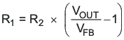
R1,R2 =
resistive divider, see Figure 5-1.
VFB = feedback voltage from the
data sheet
IR1/2 = current through the
resistive divider to GND, calculated in Equation 9
VOUT = desired output
voltage