SLVA372D November 2009 – November 2022 LM2577 , LM2585 , LM2586 , LM2587 , LM2588 , LMR61428 , LMR62014 , LMR62421 , LMR64010 , TL1451A , TL5001 , TL5001A , TLV61220 , TPS40210 , TPS40211 , TPS43000 , TPS61000 , TPS61002 , TPS61005 , TPS61006 , TPS61007 , TPS61010 , TPS61012 , TPS61013 , TPS61014 , TPS61015 , TPS61016 , TPS61020 , TPS61021A , TPS61024 , TPS61025 , TPS61026 , TPS61027 , TPS61028 , TPS61029 , TPS61029-Q1 , TPS61030 , TPS61031 , TPS61032 , TPS61046 , TPS61070 , TPS61071 , TPS61072 , TPS61073 , TPS61085 , TPS61086 , TPS61087 , TPS61088 , TPS61089 , TPS61090 , TPS61091 , TPS61092 , TPS61093 , TPS61093-Q1 , TPS61097-33 , TPS61100 , TPS61107 , TPS61120 , TPS61121 , TPS61122 , TPS61130 , TPS61131 , TPS61170 , TPS61175 , TPS61175-Q1 , TPS61200 , TPS61201 , TPS61202 , TPS61220 , TPS61221 , TPS61222 , TPS61230A , TPS61235P , TPS61236P , TPS61240 , TPS61241 , TPS61253 , TPS61254 , TPS61256 , TPS61258 , TPS61259 , TPS612592 , TPS61291 , TPS65070 , TPS65072 , TPS65073 , TPS65100 , TPS65100-Q1 , TPS65101 , TPS65105 , TPS65130 , TPS65131 , TPS65131-Q1 , TPS65132 , TPS65132S , TPS65133 , TPS65137 , TPS65140 , TPS65140-Q1 , TPS65141 , TPS65142 , TPS65145 , TPS65145-Q1 , TPS65150 , TPS65150-Q1 , TPS65154 , TPS65155 , TPS65160 , TPS65160A , TPS65161 , TPS65161A , TPS65161B , TPS65162 , TPS65163 , TPS65167A , TPS65170 , TPS65175 , TPS65175B , TPS65175C , TPS65176 , TPS65177 , TPS65177A , TPS65178 , TPS65631 , TPS65631W , TPS65632 , TPS65632A , TPS65640 , TPS65642 , TPS65642A , UCC39411
- Basic Calculation of a Boost Converter's Power Stage
- 1 Basic Configuration of a Boost Converter
- 2 Calculate the Maximum Switch Current
- 3 Inductor Selection
- 4 Rectifier Diode Selection
- 5 Output Voltage Setting
- 6 Input Capacitor Selection
- 7 Output Capacitor Selection
- 8 Equations to Calculate the Power Stage of a Boost Converter
- 9 References
- 10Revision History
7 Output Capacitor Selection
Best practice is to use low ESR capacitors to minimize the ripple on the output voltage. Ceramic capacitors are a good choice if the dielectric material is X5R or better (see reference 7 and 8).
If the converter has external compensation, any capacitor value above the recommended minimum in the data sheet can be used, but the compensation has to be adjusted for the used output capacitance.
With internally compensated converters, the recommended inductor and capacitor values should be used or the recommendations in the data sheet for adjusting the output capacitors to the application should be followed for the ratio of L × C.
With external compensation, the following equations can be used to adjust the output capacitor values for a desired output voltage ripple:
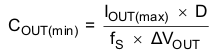
COUT(min) = minimum output capacitance
IOUT(max) = maximum output current of the application
D = duty cycle calculated with Equation 1
fS = minimum switching frequency of the converter
ΔVOUT = desired output voltage ripple
The ESR of the output capacitor adds some more ripple, given with the equation:

ΔVOUT(ESR) = additional output voltage ripple due to capacitors ESR
ESR = equivalent series resistance of the used output capacitor
IOUT(max) = maximum output current of the application
D = duty cycle calculated with Equation 1
ΔIL = inductor ripple current from Equation 2 or Equation 6