SLVA372D November 2009 – November 2022 LM2577 , LM2585 , LM2586 , LM2587 , LM2588 , LMR61428 , LMR62014 , LMR62421 , LMR64010 , TL1451A , TL5001 , TL5001A , TLV61220 , TPS40210 , TPS40211 , TPS43000 , TPS61000 , TPS61002 , TPS61005 , TPS61006 , TPS61007 , TPS61010 , TPS61012 , TPS61013 , TPS61014 , TPS61015 , TPS61016 , TPS61020 , TPS61021A , TPS61024 , TPS61025 , TPS61026 , TPS61027 , TPS61028 , TPS61029 , TPS61029-Q1 , TPS61030 , TPS61031 , TPS61032 , TPS61046 , TPS61070 , TPS61071 , TPS61072 , TPS61073 , TPS61085 , TPS61086 , TPS61087 , TPS61088 , TPS61089 , TPS61090 , TPS61091 , TPS61092 , TPS61093 , TPS61093-Q1 , TPS61097-33 , TPS61100 , TPS61107 , TPS61120 , TPS61121 , TPS61122 , TPS61131 , TPS61170 , TPS61175 , TPS61175-Q1 , TPS61200 , TPS61201 , TPS61202 , TPS61220 , TPS61221 , TPS61222 , TPS61230A , TPS61235P , TPS61236P , TPS61240 , TPS61241 , TPS61253 , TPS61254 , TPS61256 , TPS61258 , TPS61259 , TPS612592 , TPS61291 , TPS65070 , TPS65072 , TPS65073 , TPS65100 , TPS65100-Q1 , TPS65101 , TPS65105 , TPS65130 , TPS65131 , TPS65131-Q1 , TPS65132 , TPS65132S , TPS65133 , TPS65137 , TPS65140 , TPS65140-Q1 , TPS65141 , TPS65142 , TPS65145 , TPS65145-Q1 , TPS65150 , TPS65150-Q1 , TPS65154 , TPS65155 , TPS65160 , TPS65160A , TPS65161 , TPS65161A , TPS65161B , TPS65162 , TPS65163 , TPS65167A , TPS65168 , TPS65170 , TPS65175 , TPS65175B , TPS65175C , TPS65176 , TPS65177 , TPS65177A , TPS65178 , TPS65631 , TPS65631W , TPS65632 , TPS65632A , TPS65640 , TPS65642 , TPS65642A , UCC39411
- Basic Calculation of a Boost Converter's Power Stage
- 1 Basic Configuration of a Boost Converter
- 2 Calculate the Maximum Switch Current
- 3 Inductor Selection
- 4 Rectifier Diode Selection
- 5 Output Voltage Setting
- 6 Input Capacitor Selection
- 7 Output Capacitor Selection
- 8 Equations to Calculate the Power Stage of a Boost Converter
- 9 References
- 10Revision History
8 Equations to Calculate the Power Stage of a Boost Converter
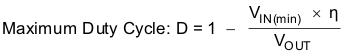
VIN(min) = minimum input
voltage
VOUT = desired output
voltage
η = efficiency of the converter, e.g.
estimated 85%
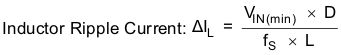
VIN(min) = minimum input
voltage
D = duty cycle calculated in Equation 14
fS = minimum switching frequency of
the converter
L = selected inductor
value

ILIM(min) = minimum value
of the current limit of the integrated witch (given in the data sheet)
ΔIL = inductor ripple current calculated
in Equation 15
D = duty cycle calculated in Equation 14

ΔIL = inductor ripple
current calculated in Equation 15
IOUT(max) = maximum output current
necessary in the application
D = duty cycle calculated
in Equation 14
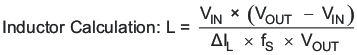
VIN = typical input
voltage
VOUT = desired output
voltage
fS = minimum switching
frequency of the converter
ΔIL= estimated
inductor ripple current, see Equation 19

ΔIL = estimated inductor
ripple current
IOUT(max) = maximum output
current necessary in the application

IOUT(max) = maximum output current necessary in the application

IF = average forward
current of the rectifier diode
VF = forward
voltage of the rectifier diode

IFB = feedback bias current from data sheet
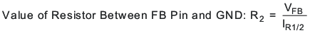
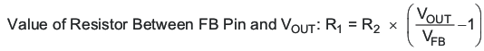
VFB = feedback voltage
from the data sheet
IR1/2 = current through
the resistive divider to GND, calculated in Equation 22
VOUT = desired output
voltage

IOUT(max) = maximum output
current of the application
D = duty cycle calculated
in Equation 14
fS = minimum switching frequency of
the converter
ΔVOUT = desired output
voltage ripple

ESR = equivalent series resistance of
the used output capacitor
IOUT(max) =
maximum output current of the application
D = duty
cycle calculated in Equation 14
ΔIL = inductor ripple current from
Equation 15 or Equation 19