SPRACV0A February 2021 – March 2023 F29H850TU , F29H850TU , F29H859TU-Q1 , F29H859TU-Q1 , TMS320F2800132 , TMS320F2800132 , TMS320F2800133 , TMS320F2800133 , TMS320F2800135 , TMS320F2800135 , TMS320F2800137 , TMS320F2800137 , TMS320F2800152-Q1 , TMS320F2800152-Q1 , TMS320F2800153-Q1 , TMS320F2800153-Q1 , TMS320F2800154-Q1 , TMS320F2800154-Q1 , TMS320F2800155 , TMS320F2800155 , TMS320F2800155-Q1 , TMS320F2800155-Q1 , TMS320F2800156-Q1 , TMS320F2800156-Q1 , TMS320F2800157 , TMS320F2800157 , TMS320F2800157-Q1 , TMS320F2800157-Q1 , TMS320F280021 , TMS320F280021 , TMS320F280021-Q1 , TMS320F280021-Q1 , TMS320F280023 , TMS320F280023 , TMS320F280023-Q1 , TMS320F280023-Q1 , TMS320F280023C , TMS320F280023C , TMS320F280025 , TMS320F280025 , TMS320F280025-Q1 , TMS320F280025-Q1 , TMS320F280025C , TMS320F280025C , TMS320F280025C-Q1 , TMS320F280025C-Q1 , TMS320F280033 , TMS320F280033 , TMS320F280034 , TMS320F280034 , TMS320F280034-Q1 , TMS320F280034-Q1 , TMS320F280036-Q1 , TMS320F280036-Q1 , TMS320F280036C-Q1 , TMS320F280036C-Q1 , TMS320F280037 , TMS320F280037 , TMS320F280037-Q1 , TMS320F280037-Q1 , TMS320F280037C , TMS320F280037C , TMS320F280037C-Q1 , TMS320F280037C-Q1 , TMS320F280038-Q1 , TMS320F280038-Q1 , TMS320F280038C-Q1 , TMS320F280038C-Q1 , TMS320F280039 , TMS320F280039 , TMS320F280039-Q1 , TMS320F280039-Q1 , TMS320F280039C , TMS320F280039C , TMS320F280039C-Q1 , TMS320F280039C-Q1 , TMS320F280040-Q1 , TMS320F280040-Q1 , TMS320F280040C-Q1 , TMS320F280040C-Q1 , TMS320F280041 , TMS320F280041 , TMS320F280041-Q1 , TMS320F280041-Q1 , TMS320F280041C , TMS320F280041C , TMS320F280041C-Q1 , TMS320F280041C-Q1 , TMS320F280045 , TMS320F280045 , TMS320F280048-Q1 , TMS320F280048-Q1 , TMS320F280048C-Q1 , TMS320F280048C-Q1 , TMS320F280049 , TMS320F280049 , TMS320F280049-Q1 , TMS320F280049-Q1 , TMS320F280049C , TMS320F280049C , TMS320F280049C-Q1 , TMS320F280049C-Q1 , TMS320F28075 , TMS320F28075 , TMS320F28075-Q1 , TMS320F28075-Q1 , TMS320F28076 , TMS320F28076 , TMS320F28374D , TMS320F28374D , TMS320F28374S , TMS320F28374S , TMS320F28375D , TMS320F28375D , TMS320F28375S , TMS320F28375S , TMS320F28375S-Q1 , TMS320F28375S-Q1 , TMS320F28376D , TMS320F28376D , TMS320F28376S , TMS320F28376S , TMS320F28377D , TMS320F28377D , TMS320F28377D-EP , TMS320F28377D-EP , TMS320F28377D-Q1 , TMS320F28377D-Q1 , TMS320F28377S , TMS320F28377S , TMS320F28377S-Q1 , TMS320F28377S-Q1 , TMS320F28378D , TMS320F28378D , TMS320F28378S , TMS320F28378S , TMS320F28379D , TMS320F28379D , TMS320F28379D-Q1 , TMS320F28379D-Q1 , TMS320F28379S , TMS320F28379S , TMS320F28384D , TMS320F28384D , TMS320F28384D-Q1 , TMS320F28384D-Q1 , TMS320F28384S , TMS320F28384S , TMS320F28384S-Q1 , TMS320F28384S-Q1 , TMS320F28386D , TMS320F28386D , TMS320F28386D-Q1 , TMS320F28386D-Q1 , TMS320F28386S , TMS320F28386S , TMS320F28386S-Q1 , TMS320F28386S-Q1 , TMS320F28388D , TMS320F28388D , TMS320F28388S , TMS320F28388S , TMS320F28P550SG , TMS320F28P550SG , TMS320F28P550SJ , TMS320F28P550SJ , TMS320F28P559SG-Q1 , TMS320F28P559SG-Q1 , TMS320F28P559SJ-Q1 , TMS320F28P559SJ-Q1 , TMS320F28P650DH , TMS320F28P650DH , TMS320F28P650DK , TMS320F28P650DK , TMS320F28P650SH , TMS320F28P650SH , TMS320F28P650SK , TMS320F28P650SK , TMS320F28P659DH-Q1 , TMS320F28P659DH-Q1 , TMS320F28P659DK-Q1 , TMS320F28P659DK-Q1 , TMS320F28P659SH-Q1 , TMS320F28P659SH-Q1
- Abstract
- Trademarks
-
1Introduction
- 1.1
Resources
- 1.1.1 TINA-TI SPICE-Based Analog Simulation Program
- 1.1.2 PSPICE for TI Design and Simulation Tool
- 1.1.3 Application Report: ADC Input Circuit Evaluation for C2000 MCUs
- 1.1.4 TI Precision Labs - SAR ADC Input Driver Design Series
- 1.1.5 Analog Engineer's Calculator
- 1.1.6 TI Precision Labs - Op Amps: Stability Series
- 1.1.7 TINA-TI ADC Input Models
- 1.1
Resources
-
2Charge-Sharing Concept
- 2.1 Traditional High-Speed ADC Driving Circuits
- 2.2 Increased Cs in High-Speed ADC Driving Circuits
- 2.3 Very Large Cs in ADC Driving Circuits
- 2.4 Charge-Sharing Operation
- 2.5 Sample Rate and Source Impedance vs. Tracking Error
- 2.6 Analytical Solution to Tracking Error
- 2.7 Charge-Sharing in Multiplexed ADCs
- 2.8 Charge-Sharing Circuit Advantages
- 2.9 Charge-Sharing Circuit Disadvantages
- 3Charge Sharing Design Flow
- 4Charge-Sharing Circuit Simulation Methods
- 5Example Circuit Designs
- 6Summary
- A Appendix: ADC Input Settling Motivation
- References
- Revision History
2.3 Very Large Cs in ADC Driving Circuits
While the previous section showed that increasing Cs results in increased settling time, there is one exception: if Cs is made sufficiently large that the second term of the equation for k (reproduced below) becomes equal to (or greater) than the first term, k will become zero (or negative) and thus the settling time, given by k⋅τ, will become zero (or negative) regardless of the size of τ. Because the predicted settling time is effectively zero, the minimum S+H duration specified in the ADC data manual can be used! When this condition is used in the design of the ADC driving circuit, the circuit is said to be using "charge-sharing".
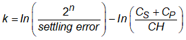
Table 2-2 shows an example of evaluating the equations under charge-sharing conditions.
| Parameter | Charge Sharing Example |
|---|---|
| CS | 102.4 nF |
| CH | 12.5 pF |
| Cp | 10 pF |
| Rs | 50 |
| RON | 425Ω |
| n | 12 bits |
| settling error | 0.5 LSBs |
| τ | 5.1 µs |
| k | 0.0 |
| Settling time | 0.0 ns |
Conceptually, the second term in the equation for k is compensating for the driver not needing to fully charge both Cs and CH. Instead, Cs is assumed to be pre-charged to the applied source voltage. This pre-charging occurs during the time when the ADC is converting and the S+H is inactive. When the S+H switch closes, the charge on Cs and CH will equalize. At the same time, the source will exponentially settle both Cs and CH towards the applied voltage. The large Cs is, the closer the voltage between Cs and CH will be to the source voltage after equalization. In the charge-sharing case, Cs is made so large that equalization alone is sufficient to get CH to within the settling error target.