SPRACY1 May 2021 F29H850TU , F29H859TU-Q1 , TMS320F2800132 , TMS320F2800133 , TMS320F2800135 , TMS320F2800137 , TMS320F2800152-Q1 , TMS320F2800153-Q1 , TMS320F2800154-Q1 , TMS320F2800155 , TMS320F2800155-Q1 , TMS320F2800156-Q1 , TMS320F2800157 , TMS320F2800157-Q1 , TMS320F280021 , TMS320F280021-Q1 , TMS320F280023 , TMS320F280023-Q1 , TMS320F280023C , TMS320F280025 , TMS320F280025-Q1 , TMS320F280025C , TMS320F280025C-Q1 , TMS320F280033 , TMS320F280034 , TMS320F280034-Q1 , TMS320F280036-Q1 , TMS320F280036C-Q1 , TMS320F280037 , TMS320F280037-Q1 , TMS320F280037C , TMS320F280037C-Q1 , TMS320F280038-Q1 , TMS320F280038C-Q1 , TMS320F280039 , TMS320F280039-Q1 , TMS320F280039C , TMS320F280039C-Q1 , TMS320F280040-Q1 , TMS320F280040C-Q1 , TMS320F280041 , TMS320F280041-Q1 , TMS320F280041C , TMS320F280041C-Q1 , TMS320F280045 , TMS320F280048-Q1 , TMS320F280048C-Q1 , TMS320F280049 , TMS320F280049-Q1 , TMS320F280049C , TMS320F280049C-Q1 , TMS320F28075 , TMS320F28075-Q1 , TMS320F28076 , TMS320F28374D , TMS320F28374S , TMS320F28375D , TMS320F28375S , TMS320F28375S-Q1 , TMS320F28376D , TMS320F28376S , TMS320F28377D , TMS320F28377D-EP , TMS320F28377D-Q1 , TMS320F28377S , TMS320F28377S-Q1 , TMS320F28378D , TMS320F28378S , TMS320F28379D , TMS320F28379D-Q1 , TMS320F28379S , TMS320F28384D , TMS320F28384D-Q1 , TMS320F28384S , TMS320F28384S-Q1 , TMS320F28386D , TMS320F28386D-Q1 , TMS320F28386S , TMS320F28386S-Q1 , TMS320F28388D , TMS320F28388S , TMS320F28P550SG , TMS320F28P550SJ , TMS320F28P559SG-Q1 , TMS320F28P559SJ-Q1 , TMS320F28P650DH , TMS320F28P650DK , TMS320F28P650SH , TMS320F28P650SK , TMS320F28P659DH-Q1 , TMS320F28P659DK-Q1 , TMS320F28P659SH-Q1
2.3.2.1 Workaround Option 1
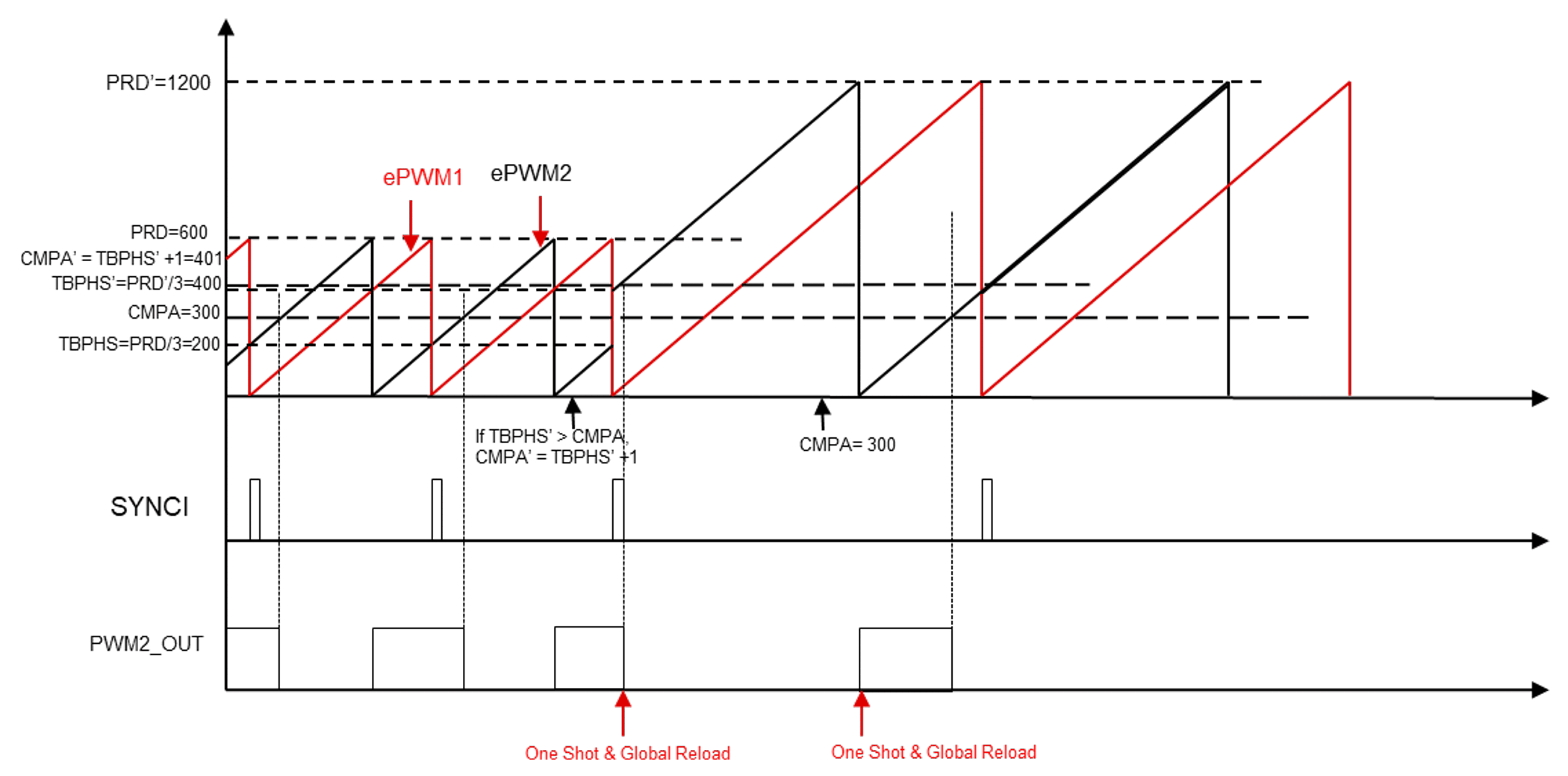
To avoid the above results, the below workaround could be an option, as shown in Figure 2-8. The global load event of ePWM1 is defined as CTR = Zero, while the global load event of ePWM2 is defined as sync event or CTR = Zero. During the ISR to update the ePWM registers, it is suggested to monitor the new CMPA and TBPHS values with their previous ones. If the new TBPHS register value and counter-compare register value will cause the PWM counter to jump over the CMPA value, the counter-compare register value can be changed temporarily, and then changed back to the required one in the next ISR.
Using the same example as above, when the new phase register TBPHS’ is updated to 400, CMPA is required to be changed to CMPA’= TBPHS’+1=401. Then, one shot load mode is enabled, so when the next global event occurs, the expected phase shift can be still maintained, while the duty cycle of ePWM2 is also clamped under the control. Then, during the next ISR, it is required to change the CMPA value back to the expected one, and also enable one shot load mode again, so that the duty cycle is corrected in the following switching cycle.
 Figure 2-8 Workaround for the Corner
Case