SPRUIF3B May 2017 – March 2019 DRA790 , DRA791 , DRA793 , DRA797
-
DRA79x EVM CPU board
- Trademarks
- 1 Introduction
- 2 Overview
- 3
Hardware
- 3.1 Hardware Architecture
- 3.2 DRA71x, DRA79x, TDA2E-17, and AM570x Processor
- 3.3 Power Architecture
- 3.4 Reset Structure
- 3.5 Clocks
- 3.6
Memory
- 3.6.1 SDRAM Memory
- 3.6.2 QSPI Flash Memory
- 3.6.3 EMMC Flash Memory
- 3.6.4 MicroSD Card Cage
- 3.6.5 GPMC NOR Flash Memory
- 3.6.6 GPMC NAND Flash Memory
- 3.6.7 Boot Modes
- 3.6.8 JTAG/Emulator and Trace
- 3.6.9 UART Terminal
- 3.6.10 DCAN and CAN Interfaces
- 3.6.11 Universal Serial Bus (USB)
- 3.6.12 Wired Ethernet
- 3.6.13 Video Output
- 3.6.14 Video Input
- 3.6.15 Mini-PCIe
- 3.6.16 Media Local Bus (MLB)
- 3.6.17 Audio
- 3.6.18 COM8 Module Interface
- 3.6.19 eFuse Programming Supply
- 3.6.20 User Interface LEDs
- 3.6.21 Power Monitoring
- 3.6.22 I2C Peripheral Map
- 3.6.23 GPIO List
- 3.6.24 I/O Expander List
- 3.6.25 Configuration EEPROM
- 4
Signal Multiplex Logic
- 4.1 GPMC and QSPI Selection (MUX A)
- 4.2 GPMC, VIN1, and VOUT3 Selection (MUX B)
- 4.3 GPMC and EMMC Selection (MUX C)
- 4.4 VIN2A and EMU Selection (MUX D, MUX E)
- 4.5 VIN2A and RGMII1 Selection (MUX F)
- 4.6 RGMII0 and VIN1B Selection (MUX J)
- 4.7 SPI2 and UART3 Selection (MUX K)
- 4.8 DCAN2 and I2C3 Selection (MUX L)
- 5 USB3 Supported Configurations
- 6 References
- Revision History
4.3 GPMC and EMMC Selection (MUX C)
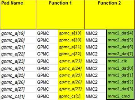
Figure 12 is part of the SoC pinmux table for GPMC. The SoC device supports additional functions not shown in the table. The functions shown are intended to reflect those supported on the EVM. These functions include:
- Memory Bus (GPMC): A[27:19]
- EMMC Memory (MMC2): CLK, CMD, D[7:0]
 Figure 12. SoC Pinmux for GPMC and EMMC
 MUX C: Selects between NOR memory and EMMC memory. The selection is made using the I/O expander 3, bits P15 and P14. If booting from EMMC, the DIP Switch SW8 position 3 is used to select interface (by default). Figure 13 shows the MUX diagram for GPMC and EMMC.
 Figure 13. MUX Diagram for GPMC and EMMC