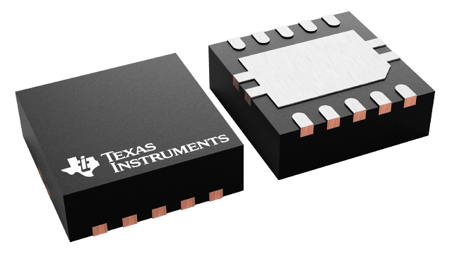
Packaging information
| Package | Pins VSON (DRC) | 10 |
| Operating temperature range (°C) -40 to 85 |
| Package qty | Carrier 250 | SMALL T&R |
Features for the TPS51103
- Wide Input Voltage Range: 4.5 V to 28 V
- 5-V/3.3-V, 100-mA, LDO Output
- Glitch Free Switch Over Circuit
- Always-On 3.3-V, 5-mA LDO Output for RTC
- 250 kHz Clock Output for Charge Pump
- Thermal Shutdown (Non-latch)
- 10Ld QFN (DRC) Package
- APPLICATIONS
- Notebook Computers
- Mobile Digital Consumer Products
Description for the TPS51103
The TPS51103 integrates three LDOs. The 5-V and 3.3-V LDOs are both rated at 100 mA and also include a glitch-free switch-over feature allowing for optimized battery life. An additional 3.3-V LDO is designed to provide an always on power output for the real time clock (RTC). The TPS51103 integrates a clock output to use with an external charge pump. The TPS51103 offers an innovative solution for optimizing the complex and multiple power rails typically found in a Notebook Computer. The TPS51103 is available in the 10-pin QFN package and is specified from –40°C to 85°C.