SN65LVDS31
- Meet or Exceed the Requirements of ANSI TIA/EIA-644 Standard
- Low-Voltage Differential Signaling With Typical Output Voltage of 350 mV and 100-Ω Load
- Typical Output Voltage Rise and Fall Times of 500 ps (400 Mbps)
- Typical Propagation Delay Times of 1.7 ns
- Operate From a Single 3.3-V Supply
- Power Dissipation 25 mW Typical Per Driver at 200 MHz
- Driver at High-Impedance When Disabled or With VCC = 0
- Bus-Terminal ESD Protection Exceeds 8 kV
- Low-Voltage TTL (LVTTL) Logic Input Levels
- Pin Compatible With AM26LS31, MC3487, and µA9638
- Cold Sparing for Space and High-Reliability Applications Requiring Redundancy
The SN55LVDS31, SN65LVDS31, SN65LVDS3487, and SN65LVDS9638 devices are differential line drivers that implement the electrical characteristics of low-voltage differential signaling (LVDS). This signaling technique lowers the output voltage levels of 5-V differential standard levels (such as TIA/EIA-422B) to reduce the power, increase the switching speeds, and allow operation with a 3.3-V supply rail. Any of the four current-mode drivers will deliver a minimum differential output voltage magnitude of 247 mV into a 100-Ω load when enabled.
관심 가지실만한 유사 제품
비교 대상 장치와 유사한 기능
기술 자료
| 상위 문서 | 유형 | 직함 | 형식 옵션 | 날짜 |
|---|---|---|---|---|
| * | Data sheet | SNx5LVDSxx High-Speed Differential Line Drivers datasheet (Rev. N) | PDF | HTML | 2021/01/21 |
| Application brief | How to Support 1.8-V Signals Using a 3.3-V LVDS Driver/Receiver + Level-Shifter | 2018/12/28 | ||
| Application brief | LVDS to Improve EMC in Motor Drives | 2018/09/27 | ||
| Application brief | How Far, How Fast Can You Operate LVDS Drivers and Receivers? | 2018/08/03 | ||
| Application note | LVDS Multidrop Connections (Rev. A) | 2002/02/11 | ||
| Application note | Performance of LVDS with Different Cables (Rev. B) | 2002/02/11 | ||
| Application note | An Overview of LVDS Technology | 1998/10/05 |
설계 및 개발
추가 조건 또는 필수 리소스는 사용 가능한 경우 아래 제목을 클릭하여 세부 정보 페이지를 확인하세요.
SN65LVDS31-32BEVM — LVDS31 및 LVDS32B용 SN65LVDS31-32BEVM 평가 모듈
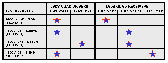
TI offers a series of low-voltage differential signaling (LVDS) evaluation modules (EVMs) designed for analysis of the electrical characteristics of LVDS drivers and receivers. Four unique EVMs are available to evaluate the different classes of LVDS devices offered by TI.
As seen (...)
SN65LVDS31-32EVM — SNx5LVDS31 및 SNx5LVDS32용 SN65LVDS31-32EVM 평가 모듈
The SN65LVDS31-32EVM evaluation moduel (EVM) includes the SV65LVDS31 quad driver and the SN65LVDS32 quad receiver. The SN65LVDS31 device is a TIA/EIA-644 standard-compliant LVDS driver. The SN65LVDS32 device is a TIA/EIA-644 standard-compliant receiver that has a passive open-circuit failsafe (...)
SN65LVDS31-33EVM — SN65LVDS31 및 SN65LVDS33용 평가 모듈
TI offers a series of low-voltage differential signaling (LVDS) evaluation modules (EVMs) designed for analysis of the electrical characteristics of LVDS drivers and receivers. Four unique EVMs are available to evaluate the different classes of LVDS devices offered by TI.
As seen in the Combination (...)
PSPICE-FOR-TI — TI 설계 및 시뮬레이션 툴용 PSpice®
TI 설계 및 시뮬레이션 환경용 PSpice는 기본 제공 라이브러리를 이용해 복잡한 혼합 신호 설계를 시뮬레이션할 수 있습니다. 레이아웃 및 제작에 착수하기 (...)
TINA-TI — SPICE 기반 아날로그 시뮬레이션 프로그램
TIDA-060017 — LVDS 인터페이스를 통한 SPI 신호 전송 레퍼런스 설계
| 패키지 | 핀 | CAD 기호, 풋프린트 및 3D 모델 |
|---|---|---|
| SOIC (D) | 16 | Ultra Librarian |
| SOP (NS) | 16 | Ultra Librarian |
| TSSOP (PW) | 16 | Ultra Librarian |
주문 및 품질
- RoHS
- REACH
- 디바이스 마킹
- 납 마감/볼 재질
- MSL 등급/피크 리플로우
- MTBF/FIT 예측
- 물질 성분
- 인증 요약
- 지속적인 신뢰성 모니터링
- 팹 위치
- 조립 위치
권장 제품에는 본 TI 제품과 관련된 매개 변수, 평가 모듈 또는 레퍼런스 디자인이 있을 수 있습니다.