SN55LVRA4-SEP
- VID V62/25606-01XE
- Total ionizing dose characterized at 30krad (Si)
- Total ionizing dose radiation lot acceptance testing (TID RLAT) for every wafer lot to 30krad (Si)
- Single-event effects (SEE) characterized:
- Single event latch-up (SEL) immune to linear energy transfer (LET) = 50MeV-cm2 /mg
- Single event transient (SET) characterization report available
- 400Mbps signaling rate
- Operates with a single 3.3V supply
- –4V to 5V extended common-mode input voltage range
- Differential input thresholds < ±50mV with 50mV of hysteresis over entire common-mode input voltage range
- Complies with TIA/EIA-644 (LVDS)
- Active fail-safe assures a high-level output with no input and input remains high-impedance on power down
- Bus-pin ESD protection exceeds 15kV HBM
- TTL control inputs are 5V tolerant
- Space enhanced plastic (SEP)
- Controlled baseline
- Gold wire, NiPdAu lead finish
- One assembly and test site, one fabrication site
- Extended product life cycle
- Military (–55°C to 125°C) temperature range
- Product traceability
- Meets NASA ASTM E595 outgassing specification
The SN55LVRA4-SEP offers the widest common-mode input voltage range in the industry. These receivers provide an input voltage range specification compatible with a 5V PECL signal as well as an overall increased ground-noise tolerance.
The SN55LVRA4-SEP include a failsafe circuit that provides a high-level output within 60ns after loss of the input signal. The most common causes of signal loss are disconnected cables, shorted lines, or powered-down transmitters. The failsafe circuit prevents noise from being received as valid data under these fault conditions.
The intended application and signaling technique of these devices is point-to-point baseband data transmission over controlled impedance media of approximately 100Ω. The transmission media can be printed-circuit board traces, backplanes, or cables. The ultimate rate and distance of data transfer is dependent upon the attenuation characteristics of the media and the noise coupling to the environment.
The SN55LVRA4-SEP is characterized for operation from –55°C to 125°C.
您可能會感興趣的類似產品
功能與所比較的裝置相似
技術文件
| 重要文件 | 類型 | 標題 | 格式選項 | 日期 |
|---|---|---|---|---|
| * | Data sheet | SN55LVRA4-SEP Radiation Tolerant Quad Channel High-Speed Differential Receiver datasheet (Rev. B) | PDF | HTML | 2026年 2月 19日 |
| * | VID | SN55LVRA4-SEP VID SN55LVRA4-SEP VID V62-25606 | 2026年 2月 20日 | |
| * | Radiation & reliability report | SN55LVRA4-SEP Total Ionizing Dose (TID) Report | 2025年 12月 10日 | |
| * | Radiation & reliability report | SN55LVRA4-SEP Single-Event Effects (SEE) Radiation Report | PDF | HTML | 2025年 12月 8日 |
| * | Radiation & reliability report | SN55LVRA4-SEP Production Flow and Reliability Report | PDF | HTML | 2025年 11月 12日 |
| Selection guide | TI Space Products (Rev. L) | 2026年 3月 27日 |
設計與開發
如需其他條款或必要資源,請按一下下方的任何標題以檢視詳細頁面 (如有)。
SN65LVDS31-33EVM — 適用 SN65LVDS31 和 SN65LVDS33 的評估模組
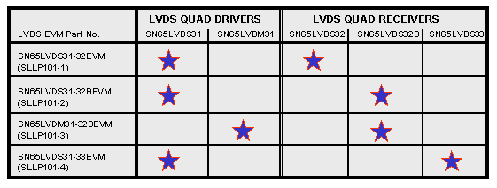
TI offers a series of low-voltage differential signaling (LVDS) evaluation modules (EVMs) designed for analysis of the electrical characteristics of LVDS drivers and receivers. Four unique EVMs are available to evaluate the different classes of LVDS devices offered by TI.
As seen in the Combination (...)
PSPICE-FOR-TI — PSpice® for TI 設計與模擬工具
PSpice for TI 設計和模擬環境可讓您使用其內建函式庫來模擬複雜的混合訊號設計。在進行佈局和製造之前,建立完整的終端設備設計和解決方案原型,進而縮短上市時間並降低開發成本。
在 PSpice for TI 設計與模擬工具中,您可以搜尋 TI (...)
TINA-TI — 基於 SPICE 的類比模擬程式
| 封裝 | 針腳 | CAD 符號、佔位空間與 3D 模型 |
|---|---|---|
| SOIC (D) | 16 | Ultra Librarian |
訂購與品質
- RoHS
- REACH
- 產品標記
- 鉛塗層/球物料
- MSL 等級/回焊峰值
- MTBF/FIT 估算值
- 材料內容
- 認證摘要
- 進行中的可靠性監測
- 晶圓廠位置
- 組裝地點
建議產品可能具有與此 TI 產品相關的參數、評估模組或參考設計。