SCAS928D May 2012 – April 2019 CDCUN1208LP
PRODUCTION DATA.
- 1 Features
- 2 Applications
- 3 Description
- 4 Revision History
- 5 Pin Configuration and Functions
-
6 Specifications
- 6.1 Absolute Maximum Ratings
- 6.2 ESD Ratings
- 6.3 Recommended Operating Conditions
- 6.4 Thermal Information
- 6.5 Digital Input Electrical Characteristics – OE (SCL), INSEL, ITTP, OTTP, Divide (SDA/MOSI), ERC(ADDR/CS), Mode
- 6.6 Universal Input (IN1, IN2) Characteristics
- 6.7 Clock Output Buffer Characteristics (Output Mode = LVDS)
- 6.8 Clock Output Buffer Characteristics (Output Mode = HCSL)
- 6.9 Clock Output Buffer Electrical Characteristics (Output Mode = LVCMOS)
- 6.10 Clock Output Buffer Electrical Characteristics (Output Mode = LVCMOS) (Continued)
- 6.11 Clock Output Buffer Electrical Characteristics (Output Mode = LVCMOS) (Continued)
- 6.12 Typical Characteristics
- 7 Parameter Measurement Information
-
8 Detailed Description
- 8.1 Overview
- 8.2 Functional Block Diagrams
- 8.3 Feature Description
- 8.4 Device Functional Modes
- 8.5
Programming
- 8.5.1
Host Interface Hardware Information
- 8.5.1.1 SPI Communication
- 8.5.1.2
I2C Communication
- 8.5.1.2.1
Message Transmission
- 8.5.1.2.1.1 Data and Address Bits
- 8.5.1.2.1.2 Special Symbols – Start (S) and Stop (P)
- 8.5.1.2.1.3 Special Symbols – Acknowledge (ACK)
- 8.5.1.2.1.4 Generic Message Frame
- 8.5.1.2.1.5 CDCUN1208LP Message Format
- 8.5.1.2.1.6 CDCUN1208LP Device Addressing (I2C Address)
- 8.5.1.2.1.7 CDCUN1208LP Device Addressing (Register Address)
- 8.5.1.2.2 I2C Master and Slave Handshaking
- 8.5.1.2.3 Block Read/Write
- 8.5.1.2.4 I2C Timing
- 8.5.1.2.1
Message Transmission
- 8.5.1
Host Interface Hardware Information
- 8.6 Register Maps
- 9 Application and Implementation
- 10Power Supply Recommendations
- 11Layout
- 12Device and Documentation Support
- 13Mechanical, Packaging, and Orderable Information
Package Options
Mechanical Data (Package|Pins)
- RHB|32
Thermal pad, mechanical data (Package|Pins)
- RHB|32
Orderable Information
3 Description
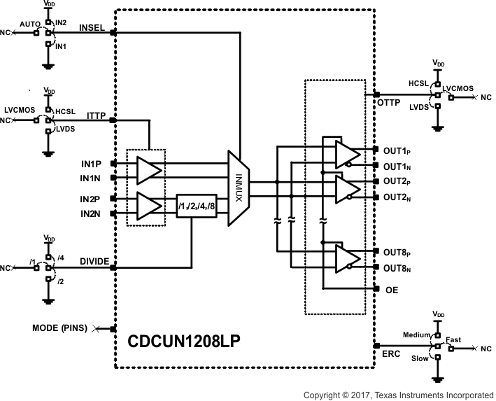
The CDCUN1208LP is a 2:8 fan-out buffer featuring a wide operating supply range, two universal differential/single-ended inputs, and universal outputs (HCSL, LVDS, or LVCMOS) with edge-rate control. The clock buffer supports PCIe Gen1, Gen2 and Gen3. One of the device inputs includes a divider that provides divide values of /1, /2, /4, or /8. The CDCUN1208LP is offered in a 32-pin QFN package, reducing the solution footprint. The device is flexible and easy to use. The state of certain pins determines device configuration at power up. Alternately, the CDCUN1208LP provides a SPI/I2C port with which a host processor controls device settings. The CDCUN1208LP delivers excellent additive jitter performance, and low power consumption. The output section includes four dedicated supply pins enabling the operation of output ports from different power supply domains. This provides the ability to clock devices switching at different LVCMOS levels without the need for external logic level translation circuitry.
Device Information(1)
| PART NUMBER | PACKAGE | BODY SIZE (NOM) |
|---|---|---|
| CDCUN1208LP | VQFN (32) | 5.00 mm × 5.00 mm |
- For all available packages, see the orderable addendum at the end of the datasheet.
Pin Configuration Overview
