SCAS928D May 2012 – April 2019 CDCUN1208LP
PRODUCTION DATA.
- 1 Features
- 2 Applications
- 3 Description
- 4 Revision History
- 5 Pin Configuration and Functions
-
6 Specifications
- 6.1 Absolute Maximum Ratings
- 6.2 ESD Ratings
- 6.3 Recommended Operating Conditions
- 6.4 Thermal Information
- 6.5 Digital Input Electrical Characteristics – OE (SCL), INSEL, ITTP, OTTP, Divide (SDA/MOSI), ERC(ADDR/CS), Mode
- 6.6 Universal Input (IN1, IN2) Characteristics
- 6.7 Clock Output Buffer Characteristics (Output Mode = LVDS)
- 6.8 Clock Output Buffer Characteristics (Output Mode = HCSL)
- 6.9 Clock Output Buffer Electrical Characteristics (Output Mode = LVCMOS)
- 6.10 Clock Output Buffer Electrical Characteristics (Output Mode = LVCMOS) (Continued)
- 6.11 Clock Output Buffer Electrical Characteristics (Output Mode = LVCMOS) (Continued)
- 6.12 Typical Characteristics
- 7 Parameter Measurement Information
-
8 Detailed Description
- 8.1 Overview
- 8.2 Functional Block Diagrams
- 8.3 Feature Description
- 8.4 Device Functional Modes
- 8.5
Programming
- 8.5.1
Host Interface Hardware Information
- 8.5.1.1 SPI Communication
- 8.5.1.2
I2C Communication
- 8.5.1.2.1
Message Transmission
- 8.5.1.2.1.1 Data and Address Bits
- 8.5.1.2.1.2 Special Symbols – Start (S) and Stop (P)
- 8.5.1.2.1.3 Special Symbols – Acknowledge (ACK)
- 8.5.1.2.1.4 Generic Message Frame
- 8.5.1.2.1.5 CDCUN1208LP Message Format
- 8.5.1.2.1.6 CDCUN1208LP Device Addressing (I2C Address)
- 8.5.1.2.1.7 CDCUN1208LP Device Addressing (Register Address)
- 8.5.1.2.2 I2C Master and Slave Handshaking
- 8.5.1.2.3 Block Read/Write
- 8.5.1.2.4 I2C Timing
- 8.5.1.2.1
Message Transmission
- 8.5.1
Host Interface Hardware Information
- 8.6 Register Maps
- 9 Application and Implementation
- 10Power Supply Recommendations
- 11Layout
- 12Device and Documentation Support
- 13Mechanical, Packaging, and Orderable Information
Package Options
Mechanical Data (Package|Pins)
- RHB|32
Thermal pad, mechanical data (Package|Pins)
- RHB|32
Orderable Information
9.3 Systems Examples
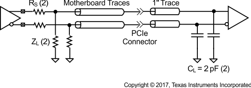
Figure 44 shows a typical application in which the receiver is off-board. The PCIe Specification (CEM2.0) requires that all source termination is on the motherboard (not on the daughter card). For this reason, the termination resistors are placed as shown. Additionally, source resistors are employed to eliminate ringing. In this case, ZL can vary between 40 Ω and 60 Ω and RS can range from 22 Ω to 33 Ω.
 Figure 44. Typical Configuration – Off-Board Receiver
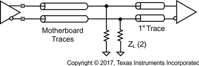
 Figure 45 shows a typical application in which the receiver is on-board. In this case, series resistors are not required to eliminate ringing as proper termination is achieved. In this case, two termination resistors, ZL = 49.9 Ω, are placed close to the receiver.
 Figure 45. Typical Configuration – On-Board Connection