SCAS928D May 2012 – April 2019 CDCUN1208LP
PRODUCTION DATA.
- 1 Features
- 2 Applications
- 3 Description
- 4 Revision History
- 5 Pin Configuration and Functions
-
6 Specifications
- 6.1 Absolute Maximum Ratings
- 6.2 ESD Ratings
- 6.3 Recommended Operating Conditions
- 6.4 Thermal Information
- 6.5 Digital Input Electrical Characteristics – OE (SCL), INSEL, ITTP, OTTP, Divide (SDA/MOSI), ERC(ADDR/CS), Mode
- 6.6 Universal Input (IN1, IN2) Characteristics
- 6.7 Clock Output Buffer Characteristics (Output Mode = LVDS)
- 6.8 Clock Output Buffer Characteristics (Output Mode = HCSL)
- 6.9 Clock Output Buffer Electrical Characteristics (Output Mode = LVCMOS)
- 6.10 Clock Output Buffer Electrical Characteristics (Output Mode = LVCMOS) (Continued)
- 6.11 Clock Output Buffer Electrical Characteristics (Output Mode = LVCMOS) (Continued)
- 6.12 Typical Characteristics
- 7 Parameter Measurement Information
-
8 Detailed Description
- 8.1 Overview
- 8.2 Functional Block Diagrams
- 8.3 Feature Description
- 8.4 Device Functional Modes
- 8.5
Programming
- 8.5.1
Host Interface Hardware Information
- 8.5.1.1 SPI Communication
- 8.5.1.2
I2C Communication
- 8.5.1.2.1
Message Transmission
- 8.5.1.2.1.1 Data and Address Bits
- 8.5.1.2.1.2 Special Symbols – Start (S) and Stop (P)
- 8.5.1.2.1.3 Special Symbols – Acknowledge (ACK)
- 8.5.1.2.1.4 Generic Message Frame
- 8.5.1.2.1.5 CDCUN1208LP Message Format
- 8.5.1.2.1.6 CDCUN1208LP Device Addressing (I2C Address)
- 8.5.1.2.1.7 CDCUN1208LP Device Addressing (Register Address)
- 8.5.1.2.2 I2C Master and Slave Handshaking
- 8.5.1.2.3 Block Read/Write
- 8.5.1.2.4 I2C Timing
- 8.5.1.2.1
Message Transmission
- 8.5.1
Host Interface Hardware Information
- 8.6 Register Maps
- 9 Application and Implementation
- 10Power Supply Recommendations
- 11Layout
- 12Device and Documentation Support
- 13Mechanical, Packaging, and Orderable Information
Package Options
Mechanical Data (Package|Pins)
- RHB|32
Thermal pad, mechanical data (Package|Pins)
- RHB|32
Orderable Information
8.3.1 Device Control Using Configuration Pins
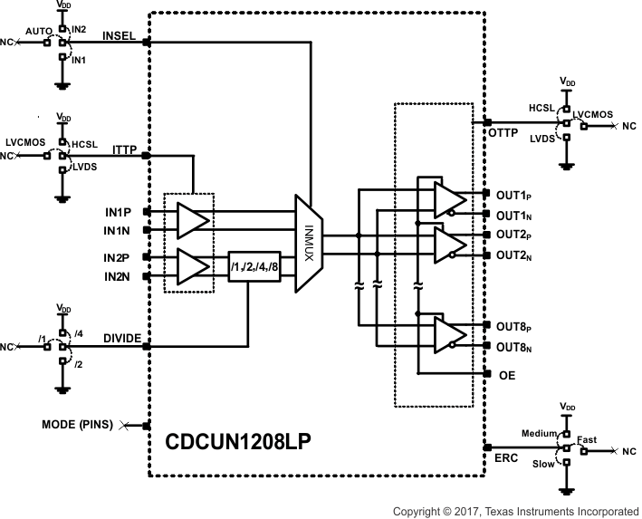
Figure 28 illustrates and Table 1 lists the CDCUN1208LP device settings using the configuration pins. Some pins sense three different states (HIGH, LOW, OPEN) according to Figure 28 and Digital Input Electrical Characteristics – OE (SCL), INSEL, ITTP, OTTP, Divide (SDA/MOSI), ERC(ADDR/CS), Mode. The device samples the state of the pins at power up and configures the device accordingly. Certain pins including INSEL and OE are sampled continuously; thus, changes of state of INSEL or OE control the device instantly.
Table 1. CDCUN1208LP Pin Configuration Summary
| PIN NAME | PIN NUMBER | DEFINITION | DEVICE CONFIGURATION DETAILS |
|---|---|---|---|
| DEVICE OUTPUTS | |||
| OTTP | 19 | Output type setting | See Table 2 |
| ERC | 31 | Edge rate control | See Table 3 |
| OE | 32 | Device global output enable | See Table 4 |
| DEVICE INPUTS | |||
| ITTP | 8 | Input type setting | See Table 5 |
| DIVIDE | 1 | IN2 input divider control | See Table 6 |
| INSEL | 2 | Input multiplexer setting | See Table 7 |
