SCAS928D May 2012 – April 2019 CDCUN1208LP
PRODUCTION DATA.
- 1 Features
- 2 Applications
- 3 Description
- 4 Revision History
- 5 Pin Configuration and Functions
-
6 Specifications
- 6.1 Absolute Maximum Ratings
- 6.2 ESD Ratings
- 6.3 Recommended Operating Conditions
- 6.4 Thermal Information
- 6.5 Digital Input Electrical Characteristics – OE (SCL), INSEL, ITTP, OTTP, Divide (SDA/MOSI), ERC(ADDR/CS), Mode
- 6.6 Universal Input (IN1, IN2) Characteristics
- 6.7 Clock Output Buffer Characteristics (Output Mode = LVDS)
- 6.8 Clock Output Buffer Characteristics (Output Mode = HCSL)
- 6.9 Clock Output Buffer Electrical Characteristics (Output Mode = LVCMOS)
- 6.10 Clock Output Buffer Electrical Characteristics (Output Mode = LVCMOS) (Continued)
- 6.11 Clock Output Buffer Electrical Characteristics (Output Mode = LVCMOS) (Continued)
- 6.12 Typical Characteristics
- 7 Parameter Measurement Information
-
8 Detailed Description
- 8.1 Overview
- 8.2 Functional Block Diagrams
- 8.3 Feature Description
- 8.4 Device Functional Modes
- 8.5
Programming
- 8.5.1
Host Interface Hardware Information
- 8.5.1.1 SPI Communication
- 8.5.1.2
I2C Communication
- 8.5.1.2.1
Message Transmission
- 8.5.1.2.1.1 Data and Address Bits
- 8.5.1.2.1.2 Special Symbols – Start (S) and Stop (P)
- 8.5.1.2.1.3 Special Symbols – Acknowledge (ACK)
- 8.5.1.2.1.4 Generic Message Frame
- 8.5.1.2.1.5 CDCUN1208LP Message Format
- 8.5.1.2.1.6 CDCUN1208LP Device Addressing (I2C Address)
- 8.5.1.2.1.7 CDCUN1208LP Device Addressing (Register Address)
- 8.5.1.2.2 I2C Master and Slave Handshaking
- 8.5.1.2.3 Block Read/Write
- 8.5.1.2.4 I2C Timing
- 8.5.1.2.1
Message Transmission
- 8.5.1
Host Interface Hardware Information
- 8.6 Register Maps
- 9 Application and Implementation
- 10Power Supply Recommendations
- 11Layout
- 12Device and Documentation Support
- 13Mechanical, Packaging, and Orderable Information
Package Options
Mechanical Data (Package|Pins)
- RHB|32
Thermal pad, mechanical data (Package|Pins)
- RHB|32
Orderable Information
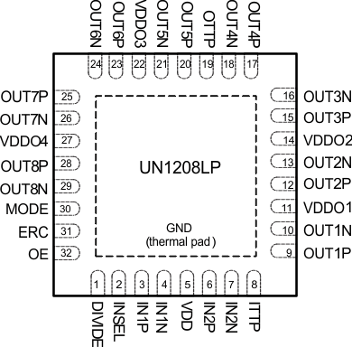
5 Pin Configuration and Functions
RHB Package
VQFN 32-Pin
Top View

Pin Functions(1)
| PIN | TYPE | DESCRIPTION | |
|---|---|---|---|
| NAME | NO. | ||
| GND | Thermal Pad | Power | Power supply ground and thermal relief |
| DIVIDE | 1 | Input | Input divider pin control
(HIGH = /4, LOW = /2, OPEN = /1) |
| INSEL | 2 | Input | Input multiplexer control |
| IN1P | 3 | Input | Universal input 1 – positive terminal |
| IN1N | 4 | Input | Universal input 1 – negative terminal, ground if using IN1 in single-ended mode |
| VDD | 5 | Power | Device power supply; provides power to the input section and clock distribution section. Use a power supply voltage that corresponds to the switching levels of clock inputs (such as 1.8 V, 2.5 V, or 3.3 V). |
| IN2P | 6 | Input | Universal input 2 – positive terminal |
| IN2N | 7 | Input | Universal input 2 – negative terminal, ground if using IN2 in single-ended mode |
| ITTP | 8 | Input | Input type select (HIGH = HCSL, LOW = LVDS, OPEN = LVCMOS) |
| OUT1P | 9 | Output | Output 1 – positive terminal |
| OUT1N | 10 | Output | Output 1 – negative terminal |
| VDDO1 | 11 | Power | Output power supply – OUT1, OUT2 |
| OUT2P | 12 | Output | Output 2 – positive terminal |
| OUT2N | 13 | Output | Output 2 – negative terminal |
| VDDO2 | 14 | Power | Output power supply – OUT3, OUT4; output bank OUT1 – OUT4 regulator power supply (apply power if any of OUT1 – OUT4 are needed) |
| OUT3P | 15 | Output | Output 3 – positive terminal |
| OUT3N | 16 | Output | Output 3 – negative terminal |
| OUT4P | 17 | Output | Output 4 – positive terminal |
| OUT4N | 18 | Output | Output 4 – negative terminal |
| OTTP | 19 | Output | Output type select (HIGH = HCSL, LOW = LVDS, OPEN = LVCMOS) |
| OUT5P | 20 | Output | Output 5 – positive terminal |
| OUT5N | 21 | Output | Output 5 – negative terminal |
| VDDO3 | 22 | Power | Output power supply - OUT5, OUT6 |
| OUT6P | 23 | Output | Output 6 – positive terminal |
| OUT6N | 24 | Output | Output 6 – negative terminal |
| OUT7P | 25 | Output | Output 7 – positive terminal |
| OUT7N | 26 | Output | Output 7 – negative terminal |
| VDDO4 | 27 | Power | Output power supply – OUT7, OUT8 output bank OUT5 – OUT8 regulator power supply (apply power if any of OUT5 – OUT8 are needed) |
| OUT8P | 28 | Output | Output 8 – positive terminal |
| OUT8N | 29 | Output | Output 8 – negative terminal |
| MODE | 30 | Input | Device control mode select
OPEN = Device configured through pins (pin mode) HIGH = Device configured through I2C LOW = Device configured through SPI Note: For information on control through the serial interface (I2C/ SPI), see Device Control Using the Host Interface section. |
| ERC | 31 | Input | Output edge rate control
HIGH = Medium, LOW = Slow, OPEN = Fast |
| OE | 32 | Input | Device output enable
HIGH = Enable, LOW = Disable |
(1) This pin list applies to operation of the device in pin mode. In host mode, certain pins take on an alternate function, as outlined in Table 8.