SCAS928D May 2012 – April 2019 CDCUN1208LP
PRODUCTION DATA.
- 1 Features
- 2 Applications
- 3 Description
- 4 Revision History
- 5 Pin Configuration and Functions
-
6 Specifications
- 6.1 Absolute Maximum Ratings
- 6.2 ESD Ratings
- 6.3 Recommended Operating Conditions
- 6.4 Thermal Information
- 6.5 Digital Input Electrical Characteristics – OE (SCL), INSEL, ITTP, OTTP, Divide (SDA/MOSI), ERC(ADDR/CS), Mode
- 6.6 Universal Input (IN1, IN2) Characteristics
- 6.7 Clock Output Buffer Characteristics (Output Mode = LVDS)
- 6.8 Clock Output Buffer Characteristics (Output Mode = HCSL)
- 6.9 Clock Output Buffer Electrical Characteristics (Output Mode = LVCMOS)
- 6.10 Clock Output Buffer Electrical Characteristics (Output Mode = LVCMOS) (Continued)
- 6.11 Clock Output Buffer Electrical Characteristics (Output Mode = LVCMOS) (Continued)
- 6.12 Typical Characteristics
- 7 Parameter Measurement Information
-
8 Detailed Description
- 8.1 Overview
- 8.2 Functional Block Diagrams
- 8.3 Feature Description
- 8.4 Device Functional Modes
- 8.5
Programming
- 8.5.1
Host Interface Hardware Information
- 8.5.1.1 SPI Communication
- 8.5.1.2
I2C Communication
- 8.5.1.2.1
Message Transmission
- 8.5.1.2.1.1 Data and Address Bits
- 8.5.1.2.1.2 Special Symbols – Start (S) and Stop (P)
- 8.5.1.2.1.3 Special Symbols – Acknowledge (ACK)
- 8.5.1.2.1.4 Generic Message Frame
- 8.5.1.2.1.5 CDCUN1208LP Message Format
- 8.5.1.2.1.6 CDCUN1208LP Device Addressing (I2C Address)
- 8.5.1.2.1.7 CDCUN1208LP Device Addressing (Register Address)
- 8.5.1.2.2 I2C Master and Slave Handshaking
- 8.5.1.2.3 Block Read/Write
- 8.5.1.2.4 I2C Timing
- 8.5.1.2.1
Message Transmission
- 8.5.1
Host Interface Hardware Information
- 8.6 Register Maps
- 9 Application and Implementation
- 10Power Supply Recommendations
- 11Layout
- 12Device and Documentation Support
- 13Mechanical, Packaging, and Orderable Information
Package Options
Mechanical Data (Package|Pins)
- RHB|32
Thermal pad, mechanical data (Package|Pins)
- RHB|32
Orderable Information
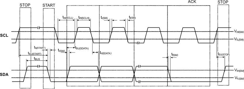
8.5.1.2.4 I2C Timing
Figure 40 and Table 10 provide details regarding the timing requirements for I2C:
 Figure 40. I2C Timing Diagram
 Table 10. I2C Timing Requirements
| PARAMETER | MIN | MAX | UNIT | |
|---|---|---|---|---|
| fSCL | SCL clock frequency | 0 | 100 | kHz |
| tsu(START) | START setup time (SCL high before SDA low) | 4.7 | µs | |
| th(START) | START hold time (SCL low after SDA low) | 4 | µs | |
| tw(SCLL) | SCL low-pulse duration | 4.7 | µs | |
| tw(SCLH) | SCL high-pulse duration | 4 | µs | |
| th(SDA) | SDA hold time (SDA valid after SCL low) | 0 | 3.45 | µs |
| tsu(SDA) | SDA setup time | 250 | ns | |
| tr | SCL / SDA input rise time | 1000 | ns | |
| tf | SCL / SDA input fall time | 300 | ns | |
| tsu(STOP) | STOP setup time | 4 | µs | |
| tBUS | Bus free time between a STOP and START condition | 4.7 | µs | |