SBOSA39A April   2025  – October 2025 THS3470

PRODUCTION DATA  

  1.   1
  2. Features
  3. Applications
  4. Description
  5. Pin Configuration and Functions
  6. Specifications
    1. 5.1 Absolute Maximum Ratings
    2. 5.2 ESD Ratings
    3. 5.3 Recommended Operating Conditions
    4. 5.4 Thermal Information
    5. 5.5 Electrical Characteristics ±VS = ±30V
    6. 5.6 Electrical Characteristics ±VS = ±20V
    7. 5.7 Typical Characteristics
  7. Detailed Description
    1. 6.1 Overview
    2. 6.2 Functional Block Diagram
    3. 6.3 Feature Description
      1. 6.3.1 Output Current Limit
      2. 6.3.2 Output Current Enable
      3. 6.3.3 Over Temperature Flag
      4. 6.3.4 Output Current Flags
      5. 6.3.5 Output Current Monitoring
      6. 6.3.6 Die Temperature Monitoring
      7. 6.3.7 External Compensation
    4. 6.4 Device Functional Modes
      1. 6.4.1 Power Modes
      2. 6.4.2 Choosing a Feedback Resistor
  8. Application and Implementation
    1. 7.1 Application Information
    2. 7.2 Typical Application
      1. 7.2.1 High-Voltage, High-Precision, Composite Amplifier
        1. 7.2.1.1 Design Requirements
        2. 7.2.1.2 Detailed Design Procedure
        3. 7.2.1.3 Application Curves
      2. 7.2.2 120V Bootstrap Amplifier
        1. 7.2.2.1 Design Requirements
        2. 7.2.2.2 Detailed Design Procedure
        3. 7.2.2.3 Application Performance Plots
    3. 7.3 Short Circuit Protection
    4. 7.4 Power Supply Recommendations
    5. 7.5 Layout
      1. 7.5.1 Thermal Considerations
        1. 7.5.1.1 Top-Side Cooling Benefits
        2. 7.5.1.2 THS3470 Safe Operating Area
      2. 7.5.2 Layout Guidelines
      3. 7.5.3 Layout Example
  9. Device and Documentation Support
    1. 8.1 Documentation Support
    2. 8.2 Receiving Notification of Documentation Updates
    3. 8.3 Support Resources
    4. 8.4 Trademarks
    5. 8.5 Electrostatic Discharge Caution
    6. 8.6 Glossary
  10. Revision History
  11. 10Mechanical, Packaging, and Orderable Information
    1. 10.1 TAPE AND REEL INFORMATION
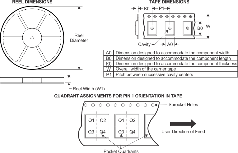
Package Options

Refer to the PDF data sheet for device specific package drawings

Mechanical Data (Package|Pins)
  • REB|42
Thermal pad, mechanical data (Package|Pins)
Orderable Information

TAPE AND REEL INFORMATION

THS3470
Device Package
Type
Package Drawing Pins SPQ Reel
Diameter (mm)
Reel
Width W1 (mm)
A0
(mm)
B0
(mm)
K0
(mm)
P1
(mm)
W
(mm)
Pin1
Quadrant
THS3470 VQFN REB 42 3000 330 16.4 7.3 7.3 1.1 12.0 16.0 Q2
THS3470
Device Package Type Package Drawing Pins SPQ Length (mm) Width (mm) Height (mm)
THS3470 VQFN REB 42 3000 367.0 367.0 38.0
THS3470
THS3470
THS3470