SLLA284G July 2022 – September 2023 ISO5451 , ISO5452 , ISO5851 , ISO5852S , ISO7142CC , ISO7142CC-Q1 , ISO721 , ISO721-Q1 , ISO721M , ISO721M-EP , ISO722 , ISO7220A , ISO7220M , ISO7221A , ISO7221B , ISO7221C , ISO7221M , ISO722M , ISO7230A , ISO7230C , ISO7230M , ISO7231A , ISO7231C , ISO7231M , ISO7240A , ISO7240C , ISO7240CF , ISO7240M , ISO7241A , ISO7241C , ISO7241M , ISO7242A , ISO7242C , ISO7242M , ISO7310-Q1 , ISO7310C , ISO7340-Q1 , ISO7340C , ISO7340FC , ISO7341-Q1 , ISO7341C , ISO7341FC , ISO7342-Q1 , ISO7342C , ISO7342FC , ISO7740 , ISO7741 , ISO7742 , ISO7760 , ISO7761 , ISO7762 , ISO7810 , ISO7820 , ISO7821 , ISO7830 , ISO7831 , ISO7840 , ISO7841 , ISO7842
4.2 Layer Stack
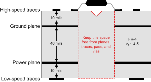
A minimum of four layers is required to accomplish a low EMI PCB design (see Figure 4-1). Layer stacking must be in the following order (top-to-bottom): high-speed signal layer, ground plane, power plane, and low-frequency signal layer.
 Figure 4-1 Recommended Layer Stack
- Routing the high-speed traces on the top layer avoids the use of vias (and the introduction of their inductances) and allows for clean interconnects between the isolator and the transmitter and receiver circuits of the data link.
- Placing a solid ground plane next to the high-speed signal layer establishes controlled impedance for transmission line interconnects and provides an excellent low-inductance path for the return current flow.
- Placing the power plane next to the ground plane creates additional high-frequency bypass capacitance of approximately 100 pF/in2.
- Routing the slower speed control signals on the bottom layer allows for greater flexibility as these signal links usually have margin to tolerate discontinuities such as vias.
If an additional supply voltage plane or signal layer is needed, add a second power/ground plane system to the stack to keep it symmetrical. This makes the stack mechanically stable and prevents it from warping. Also, the power and ground plane of each power system can be placed closer together, thus increasing the high-frequency bypass capacitance significantly.