SLLA284G July 2022 – September 2023 ISO5451 , ISO5452 , ISO5851 , ISO5852S , ISO7142CC , ISO7142CC-Q1 , ISO721 , ISO721-Q1 , ISO721M , ISO721M-EP , ISO722 , ISO7220A , ISO7220M , ISO7221A , ISO7221B , ISO7221C , ISO7221M , ISO722M , ISO7230A , ISO7230C , ISO7230M , ISO7231A , ISO7231C , ISO7231M , ISO7240A , ISO7240C , ISO7240CF , ISO7240M , ISO7241A , ISO7241C , ISO7241M , ISO7242A , ISO7242C , ISO7242M , ISO7310-Q1 , ISO7310C , ISO7340-Q1 , ISO7340C , ISO7340FC , ISO7341-Q1 , ISO7341C , ISO7341FC , ISO7342-Q1 , ISO7342C , ISO7342FC , ISO7740 , ISO7741 , ISO7742 , ISO7760 , ISO7761 , ISO7762 , ISO7810 , ISO7820 , ISO7821 , ISO7830 , ISO7831 , ISO7840 , ISO7841 , ISO7842
4.7 Vias
The term via commonly refers to a plated hole in a printed-circuit board. Although some applications require through-hole vias to be wide enough to accommodate the leads of through-hole components, high-speed board designs mainly use them as trace routing vias when changing signal layers, or as connecting vias to connect SMT components to the required reference plane, and also to connect reference planes of the same potential to each other.
Layers connecting to a via do so by making direct contact with a pad surrounding the via, (the via pad). Layers that must not connect are separated by a clearance ring. Every via has a capacitance to ground which can be approximated using the following equation:
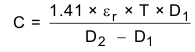
where
- D2 = diameter of clearance hole in ground planes, [in.].
- D1 = diameter of pad surround via, [in.].
- T = thickness of printed circuit board, [in.].
- εr = dielectric constant of the circuit board.
- C = parasitic via capacitance, [pF].
Because the capacitance increases proportional with size, trace vias in high-speed designs must be as small as possible to avoid signal degradation caused by heavy capacitive loading.
When connecting decoupling capacitors to a ground plane or interconnecting ground planes, the via inductance becomes more important than its capacitance. The magnitude of this inductance is approximately:
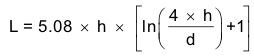
where
- L = via inductance, [nH].
- h = via length, [in.].
- d = via diameter, [in.].
Because this equation involves a logarithm, changing the via diameter does little to influence the inductance. A big change may be effected by changing the via length or by using multiple vias in parallel. Therefore, connect decoupling capacitors to ground by using two paralleled vias per device terminal. For low inductance connections between ground planes, use multiple vias in regular intervals across the board.
Although it is highly recommended not to change layers of high-speed traces, if the necessity still occurs, ensure a continuous return current path. Figure 4-13 on the left shows the flow of the return current for a single layer change and on the right for a multiple layer change.
 Figure 4-13 Return Current Paths for a Single and a Multiple Layer Change
The ability for the current flow to change from the bottom to the top of the ground plane is provided by a metallic laminate of the inner clearance ring. Thus, when a signal passes through a via and continues on the opposite side of the same plane, a return current discontinuity does not exist.
Changing a signal trace from one layer to another by crossing multiple reference planes complicates the design of the return current path. In the case of two ground planes, a ground-to-ground via must be placed near the signal via to ensure a continuous return current path, (right diagram in Figure 4-13).
If the reference planes are of different voltage potentials, such as the power and ground planes in Figure 4-14, the design of the return path becomes messy as it requires a third via and a decoupling capacitor. The return current flow begins at the bottom of the power plane, where it is closest to the signal current. It then flows through the power via, across the decoupling capacitor into the ground via and returns on top of the ground plane.
 Figure 4-14 Return Current Paths for a Single and a Multiple Layer Change
Current return paths comprising multiple vias and decoupling capacitors possess high inductance, thus compromising signal integrity and increasing EMI. If possible, avoid changing layers during high-speed trace routing, as it usually worsens board performance, complicates design, and increases manufacturing cost.