SLLA284G July 2022 – September 2023 ISO5451 , ISO5452 , ISO5851 , ISO5852S , ISO7142CC , ISO7142CC-Q1 , ISO721 , ISO721-Q1 , ISO721M , ISO721M-EP , ISO722 , ISO7220A , ISO7220M , ISO7221A , ISO7221B , ISO7221C , ISO7221M , ISO722M , ISO7230C , ISO7230M , ISO7231C , ISO7231M , ISO7240C , ISO7240CF , ISO7240M , ISO7241C , ISO7241M , ISO7242C , ISO7242M , ISO7310-Q1 , ISO7310C , ISO7340-Q1 , ISO7340C , ISO7340FC , ISO7341-Q1 , ISO7341C , ISO7341FC , ISO7342-Q1 , ISO7342C , ISO7342FC , ISO7740 , ISO7741 , ISO7742 , ISO7760 , ISO7761 , ISO7762 , ISO7810 , ISO7820 , ISO7821 , ISO7830 , ISO7831 , ISO7840 , ISO7841 , ISO7842
4.6 Routing
Guidelines for routing PCB traces and placing components are necessary when trying to maintain signal integrity, avoiding noise pick-up, and lower EMI. Although an endless number of precautions seems to be taken, this section provides only a few main recommendations as layout guidance.
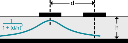
- Keep signal traces 3 times the trace-to-ground height, (d = 3h), apart to reduce crosstalk down to 10%. Because the return current density under a signal trace diminishes via a 1/ [1+(d/h)2] function, its density at a point d > 3h, is sufficiently small to avoid causing significant crosstalk in an adjacent trace.
 Figure 4-9 Separate Traces to Minimize Crosstalk
 - Use 45° bends (chamfered corners), instead of right-angle (90°) bends. Right-angle bends increase the effective trace width, and thus the trace impedance. This creates additional impedance mismatch, which may lead to higher reflections.
 Figure 4-10 Use 45° Bends Instead of 90° Bends
 - For permanent operation in noisy environments, connect the Enable inputs of an isolator through a via to the appropriate reference plane, that is, High-Enable inputs to the VCC plane and Low-Enable inputs to the ground plane.
- When routing traces next to a via or between an array of vias, ensure that the via clearance section does not interrupt the path of the return current on the ground plane below. If a via clearance section lies in the return path, the return current finds a path of least inductance around it. By doing so, it may cross below other signal traces, thus generating cross-talk and increase EMI.
 Figure 4-11 Avoiding Via Clearance Sections
 - Avoid changing layers with signal traces as this causes the inductance of the signal path to increase.
- If, however, signal trace routing over different layers is unavoidable, accompany each signal trace via with a return-trace via. In this case, use the smallest via size possible to keep the increase in inductance at a minimum.
- Use solid power and ground planes for impedance control and minimum power noise.
- Use short trace lengths between isolator and surrounding circuits to avoid noise pick-up. Digital isolators are usually accompanied by isolated dc-to-dc converters, providing supply power across the isolation barrier. Because single-ended transmission signaling is sensitive to noise pick-up, the switching frequencies of close-by dc-to-dc converters can be easily picked up by long signal traces.
- Place bulk capacitors, (i.e., 10 μF), close to power sources, such as voltage regulators or where the power is supplied to the PCB.
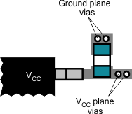
- Place smaller 0.1-μF or 0.01-μF bypass capacitors at the device by connecting the power-side of the capacitor directly to the supply terminal of the device and through two vias to the Vcc plane, and the ground-side of the capacitor through two vias to the ground plane.
 Figure 4-12 Connect Bypass Capacitor Directly to VCC Terminal