SLLA284G July 2022 – September 2023 ISO5451 , ISO5452 , ISO5851 , ISO5852S , ISO7142CC , ISO7142CC-Q1 , ISO721 , ISO721-Q1 , ISO721M , ISO721M-EP , ISO722 , ISO7220A , ISO7220M , ISO7221A , ISO7221B , ISO7221C , ISO7221M , ISO722M , ISO7230C , ISO7230M , ISO7231C , ISO7231M , ISO7240C , ISO7240CF , ISO7240M , ISO7241C , ISO7241M , ISO7242C , ISO7242M , ISO7310-Q1 , ISO7310C , ISO7340-Q1 , ISO7340C , ISO7340FC , ISO7341-Q1 , ISO7341C , ISO7341FC , ISO7342-Q1 , ISO7342C , ISO7342FC , ISO7740 , ISO7741 , ISO7742 , ISO7760 , ISO7761 , ISO7762 , ISO7810 , ISO7820 , ISO7821 , ISO7830 , ISO7831 , ISO7840 , ISO7841 , ISO7842
4.4 Controlled Impedance Transmission Lines
A controlled impedance transmission line is a trace whose characteristic impedance, Z0, is tightly controlled by the trace geometries. In general, these traces match the differential impedance of the transmission medium, such as cables and line terminators, to minimize signal reflections. Around digital isolators, controlled impedance traces must match the isolator output impedance, Z0 ~ rO, which is known as source-impedance matching.
 Figure 4-3 Source Impedance Matching: Z0 ~ rO
To determine Z0, the dynamic output impedance of the isolator, rO = ΔVOUT/ΔIOUT, needs to be established. For that purpose the output characteristic in Figure 4-4, (taken from the ISO7240 data sheet), is approximated by two linear segments indicating an rO ~ 260 Ω at low voltages, while for the majority of the curve, (and thus the transition region of the output), rO ~ 70 Ω.
 Figure 4-4 Isolator Output Characteristic
The required trace geometries, such as trace thickness (t) and width (w), the distance between trace and an adjacent ground layer (d), and the PCB dielectric (εr), are partially dictated by the copper-plating capabilities of the board manufacturing process and the dielectric of the chosen board material. Typical values are 1 and 2 oz of copper-plating, resulting in trace thicknesses of t = 1.37 mils and t = 2.74 mils, respectively. Dielectric values for FR-4 epoxy-glass vary between εr = 2.8 to 4.5 for microstrip, and εr = 4.5 for stripline traces.
With t and εr given, the designer has the freedom to define Z0 through trace width w, and distance d. For PCB designs, however, the most critical dimensions are not the absolute values of w and d, but their ratio w/d. Easing the designer’s task, Figure 4-5 plots the characteristic trace impedance as a function of the width-to-height (w/h) for a trace thickness of 2.74 mils (2-oz copper plating), an FR-4 dielectric of 4.5, and a trace-height of 10 mils above the ground plane.
 Figure 4-5 Characteristic Impedance as a Function of the w/h Ratio
From Figure 4-5 it is apparent that a 70-Ω design requires a w/h ratio of about 0.8. As described in the following section, Reference Planes, designing a low EMI board requires close electric coupling between signal trace and ground plane, which is accomplished by ensuring that h = 10 mils. The corresponding trace-width is therefore 8 mils. This width must be maintained across the entire trace length. Otherwise, variations in trace width cause discontinuities in the characteristic impedance, thus leading to increased reflections and EMI.
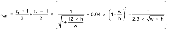
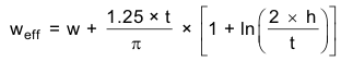
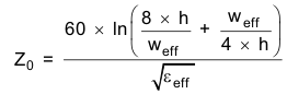
Note, that the preceding design example is only one of many possibilities to achieve the desired Z0. Different trace thickness due to higher or lower copper plating, or different PCB material can be used, but require the w/d ratio to change. The rather complex, mathematic equations for calculating the characteristic impedance Z0, while taking trace thickness, width, and dielectric into account, are presented in Table 4-1.
|
εeff =
effective dielectric, taking into account:
|
|
|
weff = effective trace width, taking into
account:
|
|
|
Z0 =
characteristic impedance, taking into account:
|
|