SLVAE30E February 2021 – March 2021 TPS1H000-Q1 , TPS1H100-Q1 , TPS1H200A-Q1 , TPS1HA08-Q1 , TPS25200-Q1 , TPS27S100 , TPS2H000-Q1 , TPS2H160-Q1 , TPS2HB16-Q1 , TPS2HB35-Q1 , TPS2HB50-Q1 , TPS4H000-Q1 , TPS4H160-Q1
- Trademarks
- 1Introduction
- 2Driving Resistive Loads
- 3Driving Capacitive Loads
- 4Driving Inductive Loads
- 5Driving LED Loads
- 6Appendix
- 7References
- 8Revision History
3.3.1 Capacitive Load Charging
When a voltage is applied to an uncharged capacitor the capacitor will sink current until it’s voltage is equal to the supply voltage. The magnitude of the inrush current is directly proportional to the rate at which the voltage across the capacitor changes with time. The resulting inrush current can be calculated by Equation 16 and be seen in Figure 3-3.
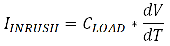
 Figure 3-3 Capacitive Load Charging Diagram
When the switch is closed and the voltage is first applied to the capacitor, dV/dT is determined by the rate at which the switch in Figure 3-3 ramps up the output voltage. Depending on this rate the inrush can be very high and would only be limited by the parasitic resistance and inductance present in the routing between the switch output and the capacitor. Without anything limiting IINRUSH, these high currents can lead to a voltage supply droop at the input voltage supply which could collapse due to the high level of power required. This can be seen in Figure 3-4, where charging a capacitor with a high dV/dT leads to inrush currents up to a peak of 40 A and causes a noticeable drop on the yellow input supply voltage.
 Figure 3-4 Inrush Supply Droop Example
This input supply drop means that any other systems connected to the same voltage supply must be able to operate without any variation even with an unstable supply. Additionally, the 40 A of current itself causes problems as the system must now be analyzed to make sure that there won’t be any harm caused by the excessive current flow through the cables and connectors. This means more complex and expensive systems in the form of:
- Larger traces and connectors to accommodate the large current
- More powerful supply to prevent the supply droop
- Increased bulk capacitors at the input of downstream systems to enable continued device operation
To prevent these system considerations it is necessary to have a solution in place to let the system drive the capacitor and charge it at a controlled rate without allowing it to sink high levels of inrush current. In the next section we will show how this can be done with an adjustable current-limiting Smart High Side Switch.