SPRACW9A June 2021 – March 2023 F29H850TU , F29H850TU , F29H859TU-Q1 , F29H859TU-Q1 , TMS320F2800132 , TMS320F2800132 , TMS320F2800133 , TMS320F2800133 , TMS320F2800135 , TMS320F2800135 , TMS320F2800137 , TMS320F2800137 , TMS320F2800152-Q1 , TMS320F2800152-Q1 , TMS320F2800153-Q1 , TMS320F2800153-Q1 , TMS320F2800154-Q1 , TMS320F2800154-Q1 , TMS320F2800155 , TMS320F2800155 , TMS320F2800155-Q1 , TMS320F2800155-Q1 , TMS320F2800156-Q1 , TMS320F2800156-Q1 , TMS320F2800157 , TMS320F2800157 , TMS320F2800157-Q1 , TMS320F2800157-Q1 , TMS320F280021 , TMS320F280021 , TMS320F280021-Q1 , TMS320F280021-Q1 , TMS320F280023 , TMS320F280023 , TMS320F280023-Q1 , TMS320F280023-Q1 , TMS320F280023C , TMS320F280023C , TMS320F280025 , TMS320F280025 , TMS320F280025-Q1 , TMS320F280025-Q1 , TMS320F280025C , TMS320F280025C , TMS320F280025C-Q1 , TMS320F280025C-Q1 , TMS320F280033 , TMS320F280033 , TMS320F280034 , TMS320F280034 , TMS320F280034-Q1 , TMS320F280034-Q1 , TMS320F280036-Q1 , TMS320F280036-Q1 , TMS320F280036C-Q1 , TMS320F280036C-Q1 , TMS320F280037 , TMS320F280037 , TMS320F280037-Q1 , TMS320F280037-Q1 , TMS320F280037C , TMS320F280037C , TMS320F280037C-Q1 , TMS320F280037C-Q1 , TMS320F280038-Q1 , TMS320F280038-Q1 , TMS320F280038C-Q1 , TMS320F280038C-Q1 , TMS320F280039 , TMS320F280039 , TMS320F280039-Q1 , TMS320F280039-Q1 , TMS320F280039C , TMS320F280039C , TMS320F280039C-Q1 , TMS320F280039C-Q1 , TMS320F280040-Q1 , TMS320F280040-Q1 , TMS320F280040C-Q1 , TMS320F280040C-Q1 , TMS320F280041 , TMS320F280041 , TMS320F280041-Q1 , TMS320F280041-Q1 , TMS320F280041C , TMS320F280041C , TMS320F280041C-Q1 , TMS320F280041C-Q1 , TMS320F280045 , TMS320F280045 , TMS320F280048-Q1 , TMS320F280048-Q1 , TMS320F280048C-Q1 , TMS320F280048C-Q1 , TMS320F280049 , TMS320F280049 , TMS320F280049-Q1 , TMS320F280049-Q1 , TMS320F280049C , TMS320F280049C , TMS320F280049C-Q1 , TMS320F280049C-Q1 , TMS320F28075 , TMS320F28075 , TMS320F28075-Q1 , TMS320F28075-Q1 , TMS320F28076 , TMS320F28076 , TMS320F28374D , TMS320F28374D , TMS320F28374S , TMS320F28374S , TMS320F28375D , TMS320F28375D , TMS320F28375S , TMS320F28375S , TMS320F28375S-Q1 , TMS320F28375S-Q1 , TMS320F28376D , TMS320F28376D , TMS320F28376S , TMS320F28376S , TMS320F28377D , TMS320F28377D , TMS320F28377D-EP , TMS320F28377D-EP , TMS320F28377D-Q1 , TMS320F28377D-Q1 , TMS320F28377S , TMS320F28377S , TMS320F28377S-Q1 , TMS320F28377S-Q1 , TMS320F28378D , TMS320F28378D , TMS320F28378S , TMS320F28378S , TMS320F28379D , TMS320F28379D , TMS320F28379D-Q1 , TMS320F28379D-Q1 , TMS320F28379S , TMS320F28379S , TMS320F28384D , TMS320F28384D , TMS320F28384D-Q1 , TMS320F28384D-Q1 , TMS320F28384S , TMS320F28384S , TMS320F28384S-Q1 , TMS320F28384S-Q1 , TMS320F28386D , TMS320F28386D , TMS320F28386D-Q1 , TMS320F28386D-Q1 , TMS320F28386S , TMS320F28386S , TMS320F28386S-Q1 , TMS320F28386S-Q1 , TMS320F28388D , TMS320F28388D , TMS320F28388S , TMS320F28388S , TMS320F28P650DH , TMS320F28P650DH , TMS320F28P650DK , TMS320F28P650DK , TMS320F28P650SH , TMS320F28P650SH , TMS320F28P650SK , TMS320F28P650SK , TMS320F28P659DH-Q1 , TMS320F28P659DH-Q1 , TMS320F28P659DK-Q1 , TMS320F28P659DK-Q1 , TMS320F28P659SH-Q1 , TMS320F28P659SH-Q1
- Abstract
- Trademarks
-
1Introduction
- 1.1 Memory Cross-Talk Challenges
- 1.2
Resources for Signal Conditioning Circuit
Design
- 1.2.1 TI Precision Labs - SAR ADC Input Driver Design Series
- 1.2.2 Analog Engineer's Calculator
- 1.2.3 Related Application Reports
- 1.2.4 TINA-TI SPICE-Based Analog Simulation Program
- 1.2.5 PSPICE for TI
- 1.2.6 ADC Input Circuit Evaluation for C2000 MCUs
- 1.2.7 Charge-Sharing Driving Circuits for C2000 ADCs
- 2Review of ADC Input Settling
- 3Problem Statement
- 4Dedicated ADC Sampling
- 5Pre-Sampling VREFLO
- 6Summary
- 7References
- 8Revision History
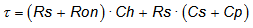
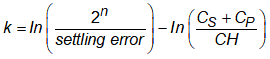
3.2 S+H Settling Analysis
As presented in Charge-Sharing Driving Circuits for C2000 ADCs, an approximation of the required settling time can be determined using an RC settling model. The time constant for the model is given by the equation:
And the number of time constants needed is given by the equation:
So the total S+H time should be set to approximately:

Where the following parameters are provided by the ADC input model in the device-specific data manual:
- n = ADC resolution (in bits)
- RON = ADC sampling switch resistance (in Ohms)
- CH = ADC sampling capacitor (in pF)
- CP = ADC channel parasitic input capacitance (in pF)
The following parameters are dependent on the application design:
- Settling error = tolerable settling error (in LSBs)
- Rs = ADC driving circuit source impedance (in Ω)
- CS = capacitance on ADC input pin (in pF)
Table 3-1 shows the settling time calculation using the values from the F280049 data manual and 250pF for CS. Rs is set to 7444Ω, which is the effective impedance of the voltage divider formed by the 1MΩ and 7.5 kΩ resistors (1MΩ || 7.5 kΩ).
| Parameter | Example 1 |
|---|---|
| CS | 250 pF |
| CH | 12.5 pF |
| Cp | 10 pF |
| Rs |
7444Ω |
| RON | 500Ω |
| n | 12 bits |
| settling error |
0.5 LSBs |
| τ | 1.96 µs |
| k |
6.015 |
| Settling time | 11.8 µs |
This analysis indicates that a settling time of 11.8 µs would be needed to achieve full 12-bit settling performance. This is, unfortunately, much longer than the maximum S+H time that the F280049 device's ADCs can be configured for. Furthermore, this is even longer than the 10 µs triggering period resulting from the 100 kHz ePWM trigger source. The latency resulting from such a long S+H window is also likely to be quite detrimental to the control system's performance. Overall, it will not be possible to get good settling performance just by configuring the correct S+H time.
Figure 3-3 shows the results of simulating Figure 3-2 while setting the S+H time to 100 ns. This time is much less than the 11.8 µs estimated to give full 12-bit settling performance, but represents what might be reasonably configured given the 100 kHz sample rate and a desire for low latency sampling. The simulation shows 131 mV of settling error after the 100 ns S+H window, which is about 4% of the ADC's 3.0 V range. This is quite poor performance considering that an ideal 12-bit ADC is capable of resolving steps of about 0.02% of the ADC's full-scale range.
 Figure 3-3 Settling
Simulation for V2 Circuit With 100 ns S+H
Figure 3-3 Settling
Simulation for V2 Circuit With 100 ns S+H