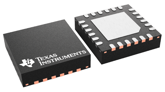
Packaging information
| Package | Pins VQFN (RGE) | 24 |
| Operating temperature range (°C) -40 to 105 |
| Package qty | Carrier 3,000 | LARGE T&R |
Features for the TPS65131-Q1
- Qualified for automotive applications
- AEC-Q100 test guidance with the following
results:
- Device temperature grade 2: –40°C to 105°C ambient operating temperature range
- Electrical characteristics tested over –40°C to 125°C junction temperature range
- Device HBM ESD classification level H1C
- Device CDM ESD classification level C4B
- Dual adjustable output voltages up to 15V and down to –15V
- 2A typical switch-current limit for boost and inverter main switches
- High conversion efficiency
- Up to 91% at positive output rail
- Up to 85% at negative output rail
- Power-save mode at low load
- Independent enable inputs for power-up and power-down Sequencing
- Control output for external PFET to support complete supply Disconnect When Shut Down
- 2.7V to 5.5V input-voltage range
- Minimum 1.25MHz fixed-frequency PWM operation
- Thermal shutdown
- Overvoltage protection on both outputs
- 0.2µA typical shutdown current
- Small 4mm × 4mm QFN-24 package (RGE) with wettable flanks
Description for the TPS65131-Q1
The TPS65131-Q1 device is dual-output dc-dc converter generating a positive output voltage up to 15V and a negative output voltage down to –15V with output currents of typically 200mA, depending on input-voltage to output-voltage ratio. With a total efficiency up to 85%, the device is ideal for portable battery-powered equipment. The input-voltage range of 2.7V to 5.5V allows, for example, 3.3V and 5V rails to power the TPS65131-Q1 device. The TPS65131-Q1 device comes in a QFN-24 package with thermal pad and wettable flanks. Requiring few and small external components, the overall solution size can be small.
The converter operates with a fixed-frequency PWM control topology and, with power-save mode enabled, uses a pulse-skipping mode at light load currents. In operation, the typical overall device quiescent current is only 500µA. In shutdown, the device draws typically 0.2µA. Independent enable pins allow power-up and power-down sequencing for both outputs. The device has an internal current limit, overvoltage protection, and a thermal shutdown for highest reliability under fault conditions.
The TPS65131-Q1 device is qualified for automotive applications, according to AEC-Q100 temperature grade 2. The electrical characteristics are tested over –40°C to 125°C device junction temperature. This, combined with lowest shutdown currents, small solution size, package with thermal pad, plus good efficiency and protection features, targets automotive and industrial applications.