JAJSFA9E November 2011 – April 2018 ADS5294
PRODUCTION DATA.
- 1 特長
- 2 アプリケーション
- 3 概要
- 4 改訂履歴
- 5 概要(続き)
- 6 デバイス比較表
- 7 Pin Configuration and Functions
-
8 Specifications
- 8.1 Absolute Maximum Ratings
- 8.2 ESD Ratings
- 8.3 Recommended Operating Conditions
- 8.4 Thermal Information
- 8.5 Electrical Characteristics Dynamic Performance
- 8.6 Digital Characteristics
- 8.7 Timing Requirements
- 8.8 LVDS Timing at Different Sampling Frequencies — 2-Wire Interface, 7x-Serialization, Digital Filter Disabled
- 8.9 LVDS Timing at Different Sampling Frequencies — 1-Wire Interface, 14x-Serialization, Digital Filter Disabled
- 8.10 Serial Interface Timing Requirements
- 8.11 Reset Timing
- 8.12 LVDS Timing at Different Sampling Frequencies — 1-Wire Interface, 14x-Serialization, Decimation by 2 Filter Enabled
- 8.13 LVDS Timing at Different Sampling Frequencies — 1-Wire Interface, 14x-Serialization, Decimation by 4 Filter Enabled
- 8.14 LVDS Timing at Different Sampling Frequencies — 1-Wire Interface, 14x-Serialization, Decimation by 8 Filter Enabled
- 8.15 Typical Characteristics
-
9 Detailed Description
- 9.1 Overview
- 9.2 Functional Block Diagram
- 9.3 Feature Description
- 9.4 Device Functional Modes
- 9.5 Programming
- 9.6
Register Maps
- 9.6.1
Description Of Serial Registers
- 9.6.1.1 Power-Down Modes
- 9.6.1.2 Low Frequency Noise Suppression Mode
- 9.6.1.3 Analog Input Invert
- 9.6.1.4 LVDS Test Patterns
- 9.6.1.5 Bit-Byte-Word Wise Output
- 9.6.1.6 Digital Processing Blocks
- 9.6.1.7 Programmable Digital Gain
- 9.6.1.8 Channel Averaging
- 9.6.1.9 Decimation Filter
- 9.6.1.10 Highpass Filter
- 9.6.1.11 Bit-Clock Programmability
- 9.6.1.12 Output Data Rate Control
- 9.6.1.13 Synchronization Pulse
- 9.6.1.14 External Reference Mode of Operation
- 9.6.1.15 Data Output Format Modes
- 9.6.1.16 Programmable Mapping Between Input Channels and Output Pins
- 9.6.1
Description Of Serial Registers
- 10Application and Implementation
- 11Power Supply Recommendations
- 12Layout
- 13デバイスおよびドキュメントのサポート
- 14メカニカル、パッケージ、および注文情報
パッケージ・オプション
メカニカル・データ(パッケージ|ピン)
- PFP|80
サーマルパッド・メカニカル・データ
- PFP|80
発注情報
8.9 LVDS Timing at Different Sampling Frequencies — 1-Wire Interface, 14x-Serialization, Digital Filter Disabled
See (1)| ADC CLK Frequency (MSPS) | Set-up Time (tsu), ns | Hold Time (tH), ns | tPROG = (5 / 7) × T + tdelay, ns(2) | ||||||
|---|---|---|---|---|---|---|---|---|---|
| Fs = 1 / T | Data Valid to Zero-Crossing of LCLKP
(both edges) |
Zero-Crossing of LCLKP to Data Becoming Invalid
(both edges) |
tPROG = delay from Input clock zero-cross rising edge to frame clock zero cross (rising edge) | ||||||
| MIN | TYP | MAX | MIN | TYP | MAX | MIN | TYP | MAX | |
| 50 | 0.28 | 0.48 | 0.28 | 0.6 | 7.5 | 9 | 10.5 | ||
| 40 | 0.5 | 0.68 | 0.54 | 0.8 | 7.5 | 9 | 10.5 | ||
| 30 | 0.62 | 0.8 | 1 | 1.25 | 7.5 | 9 | 10.5 | ||
| 20 | 1.2 | 1.4 | 1.6 | 1.9 | 7.5 | 9 | 10.5 | ||
| 10 | 3.1 | 3.3 | 3.3 | 3.5 | 7.5 | 9 | 10.5 | ||
NOTE
The LVDS timing specification is only valid when digital decimation filters are disabled. When digital filters are enabled, the set-up time decreases as the corresponding hold time increases as shown in LVDS Timing at Different Sampling Frequencies — 1-Wire Interface, 14x-Serialization, Decimation by 2 Filter Enabled to LVDS Timing at Different Sampling Frequencies — 1-Wire Interface, 14x-Serialization, Decimation by 8 Filter Enabled. The change on LVDS timing also depends on the internal PLL setting of the ADS5294. See PLL Operation Versus LVDS Timing for more information.
At the highest sampling frequency, 80-MSPS, and decimation of 2 ( for example: effective data rate = 560 Mbps in 1-wire mode), the set-up time is reduced by 70 ps, (for example: set-up time, min = 0.43 ns; hold time, min = 0.54 ns). scenario assumes that the recommended PLL settings are configured as shown in PLL Operation Versus LVDS Timing
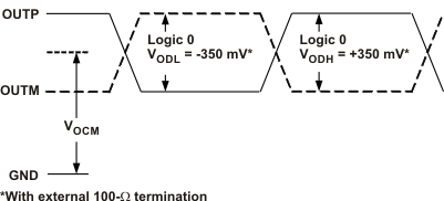 Figure 2. LVDS Output Voltage Levels
 Figure 3. 14-Bit 1-Wire LVDS Timing Diagram
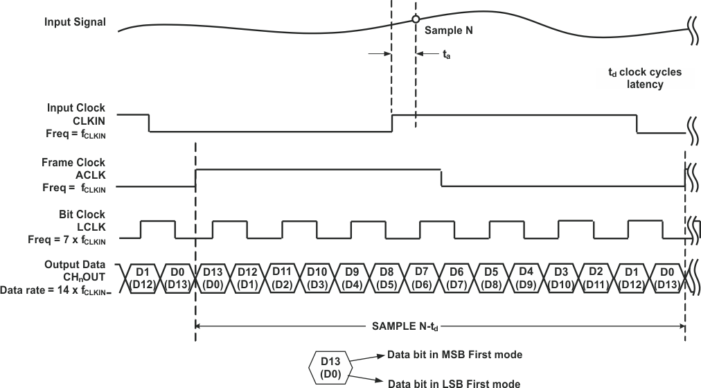 Figure 4. Enlarged 1-Wire LVDS Timing Diagram (14 bit)
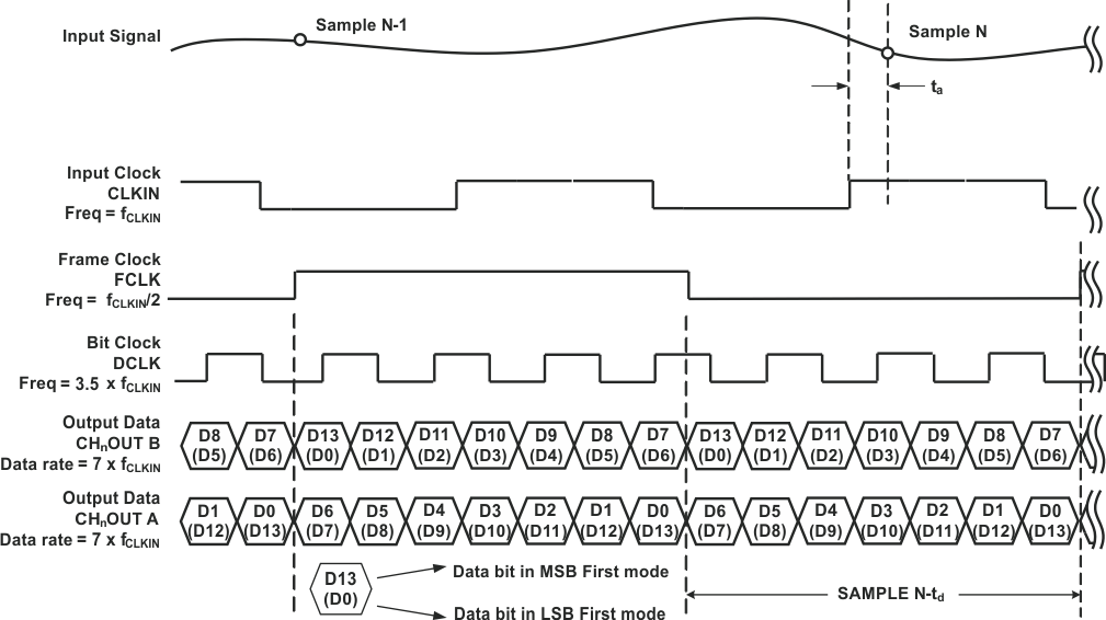 Figure 6. Enlarged 2-Wire LVDS Timing Diagram (14 bit)
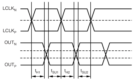 Figure 7. Definition of Setup and Hold Times tSU = min(tSU1, tSU2); tH = min(tH1, tH2)
