JAJSFA9E November 2011 – April 2018 ADS5294
PRODUCTION DATA.
- 1 特長
- 2 アプリケーション
- 3 概要
- 4 改訂履歴
- 5 概要(続き)
- 6 デバイス比較表
- 7 Pin Configuration and Functions
-
8 Specifications
- 8.1 Absolute Maximum Ratings
- 8.2 ESD Ratings
- 8.3 Recommended Operating Conditions
- 8.4 Thermal Information
- 8.5 Electrical Characteristics Dynamic Performance
- 8.6 Digital Characteristics
- 8.7 Timing Requirements
- 8.8 LVDS Timing at Different Sampling Frequencies — 2-Wire Interface, 7x-Serialization, Digital Filter Disabled
- 8.9 LVDS Timing at Different Sampling Frequencies — 1-Wire Interface, 14x-Serialization, Digital Filter Disabled
- 8.10 Serial Interface Timing Requirements
- 8.11 Reset Timing
- 8.12 LVDS Timing at Different Sampling Frequencies — 1-Wire Interface, 14x-Serialization, Decimation by 2 Filter Enabled
- 8.13 LVDS Timing at Different Sampling Frequencies — 1-Wire Interface, 14x-Serialization, Decimation by 4 Filter Enabled
- 8.14 LVDS Timing at Different Sampling Frequencies — 1-Wire Interface, 14x-Serialization, Decimation by 8 Filter Enabled
- 8.15 Typical Characteristics
-
9 Detailed Description
- 9.1 Overview
- 9.2 Functional Block Diagram
- 9.3 Feature Description
- 9.4 Device Functional Modes
- 9.5 Programming
- 9.6
Register Maps
- 9.6.1
Description Of Serial Registers
- 9.6.1.1 Power-Down Modes
- 9.6.1.2 Low Frequency Noise Suppression Mode
- 9.6.1.3 Analog Input Invert
- 9.6.1.4 LVDS Test Patterns
- 9.6.1.5 Bit-Byte-Word Wise Output
- 9.6.1.6 Digital Processing Blocks
- 9.6.1.7 Programmable Digital Gain
- 9.6.1.8 Channel Averaging
- 9.6.1.9 Decimation Filter
- 9.6.1.10 Highpass Filter
- 9.6.1.11 Bit-Clock Programmability
- 9.6.1.12 Output Data Rate Control
- 9.6.1.13 Synchronization Pulse
- 9.6.1.14 External Reference Mode of Operation
- 9.6.1.15 Data Output Format Modes
- 9.6.1.16 Programmable Mapping Between Input Channels and Output Pins
- 9.6.1
Description Of Serial Registers
- 10Application and Implementation
- 11Power Supply Recommendations
- 12Layout
- 13デバイスおよびドキュメントのサポート
- 14メカニカル、パッケージ、および注文情報
パッケージ・オプション
メカニカル・データ(パッケージ|ピン)
- PFP|80
サーマルパッド・メカニカル・データ
- PFP|80
発注情報
9.3.6 PLL Operation Versus LVDS Timing
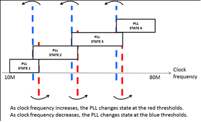
The ADS5294 uses a PLL that automatically changes configuration to one of four states depending on the sampling clock frequency. The clock frequency detection is automatic and each time the sampling frequency crosses a threshold, the PLL changes configuration to a new state. The PLL remains in the new state for a range of clock frequencies. To prevent unwanted toggling of PLL state around a threshold, the circuit has an built-in hysteresis. The ADS5294 has three thresholds over the sampling clock frequency range from 10 MHz to 80 MHz and can be in one of four states as shown by Figure 50.
 Figure 50. PLL States Versus ADC Fs
Each threshold shifts by a small amount across temperature. On power up, depending on the clock frequency, the PLL settles in one of four states. Later, as the system warms up, the PLL changes state once due to the shift in the threshold across temperature.