JAJSFA9E November 2011 – April 2018 ADS5294
PRODUCTION DATA.
- 1 特長
- 2 アプリケーション
- 3 概要
- 4 改訂履歴
- 5 概要(続き)
- 6 デバイス比較表
- 7 Pin Configuration and Functions
-
8 Specifications
- 8.1 Absolute Maximum Ratings
- 8.2 ESD Ratings
- 8.3 Recommended Operating Conditions
- 8.4 Thermal Information
- 8.5 Electrical Characteristics Dynamic Performance
- 8.6 Digital Characteristics
- 8.7 Timing Requirements
- 8.8 LVDS Timing at Different Sampling Frequencies — 2-Wire Interface, 7x-Serialization, Digital Filter Disabled
- 8.9 LVDS Timing at Different Sampling Frequencies — 1-Wire Interface, 14x-Serialization, Digital Filter Disabled
- 8.10 Serial Interface Timing Requirements
- 8.11 Reset Timing
- 8.12 LVDS Timing at Different Sampling Frequencies — 1-Wire Interface, 14x-Serialization, Decimation by 2 Filter Enabled
- 8.13 LVDS Timing at Different Sampling Frequencies — 1-Wire Interface, 14x-Serialization, Decimation by 4 Filter Enabled
- 8.14 LVDS Timing at Different Sampling Frequencies — 1-Wire Interface, 14x-Serialization, Decimation by 8 Filter Enabled
- 8.15 Typical Characteristics
-
9 Detailed Description
- 9.1 Overview
- 9.2 Functional Block Diagram
- 9.3 Feature Description
- 9.4 Device Functional Modes
- 9.5 Programming
- 9.6
Register Maps
- 9.6.1
Description Of Serial Registers
- 9.6.1.1 Power-Down Modes
- 9.6.1.2 Low Frequency Noise Suppression Mode
- 9.6.1.3 Analog Input Invert
- 9.6.1.4 LVDS Test Patterns
- 9.6.1.5 Bit-Byte-Word Wise Output
- 9.6.1.6 Digital Processing Blocks
- 9.6.1.7 Programmable Digital Gain
- 9.6.1.8 Channel Averaging
- 9.6.1.9 Decimation Filter
- 9.6.1.10 Highpass Filter
- 9.6.1.11 Bit-Clock Programmability
- 9.6.1.12 Output Data Rate Control
- 9.6.1.13 Synchronization Pulse
- 9.6.1.14 External Reference Mode of Operation
- 9.6.1.15 Data Output Format Modes
- 9.6.1.16 Programmable Mapping Between Input Channels and Output Pins
- 9.6.1
Description Of Serial Registers
- 10Application and Implementation
- 11Power Supply Recommendations
- 12Layout
- 13デバイスおよびドキュメントのサポート
- 14メカニカル、パッケージ、および注文情報
パッケージ・オプション
メカニカル・データ(パッケージ|ピン)
- PFP|80
サーマルパッド・メカニカル・データ
- PFP|80
発注情報
8.15 Typical Characteristics
Typical values are at 25°C, AVDD = 1.8 V, LVDD = 1.8 V, 50% clock duty cycle, –1-dBFS differential analog input, 14 Bit/ 80 MSPS, ADC is configured in the internal reference mode, unless otherwise noted.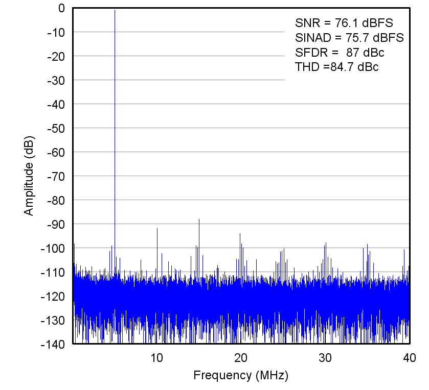 Figure 8. FFT for 5-MHz Input Signal, Sample Rate = 80 MSPS
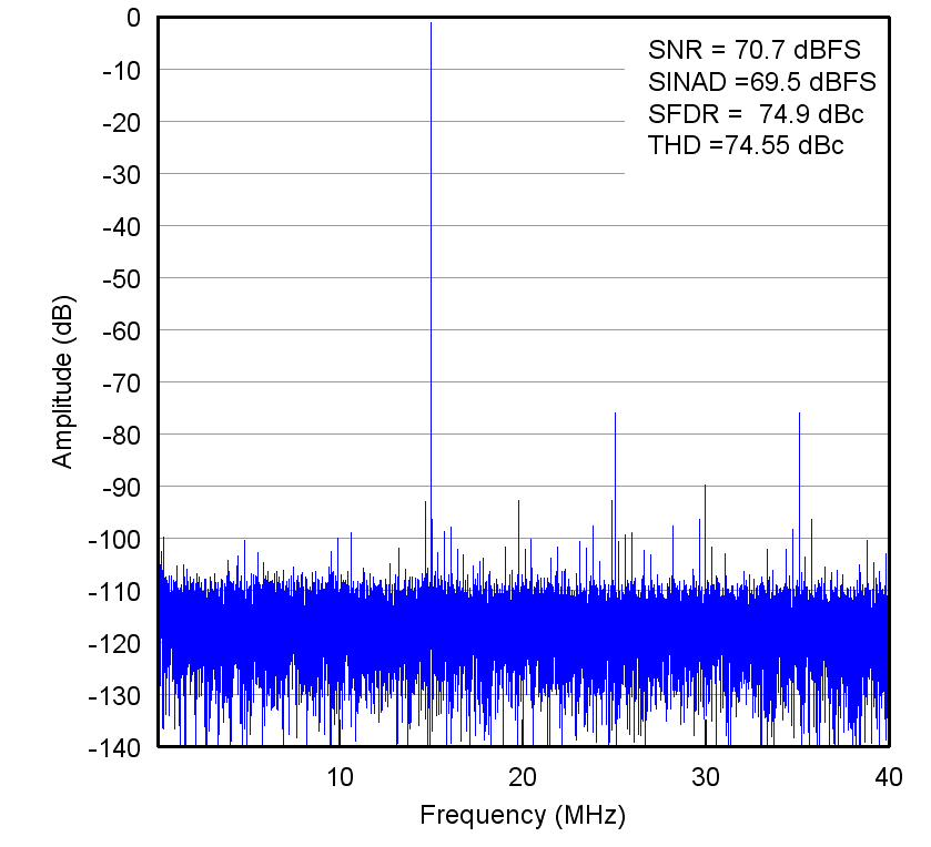 Figure 10. FFT for 65-MHz Input Signal, Sample Rate = 80 MSPS
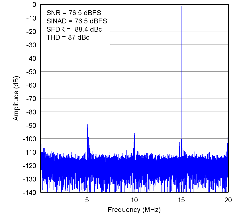 Figure 12. FFT for 15-MHz Input Signal, Sample Rate = 40 MSPS
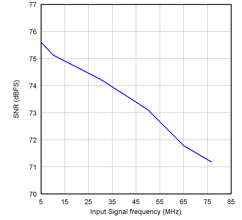 Figure 14. Signal-To-Noise Ratio vs Input Signal Frequency
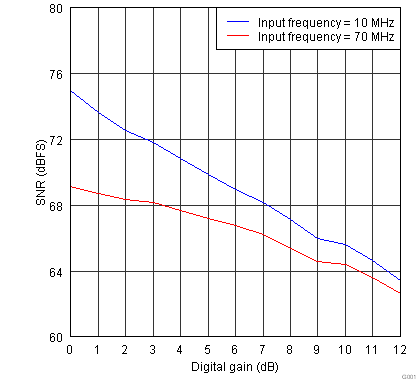 Figure 16. SNR vs Digital Gain
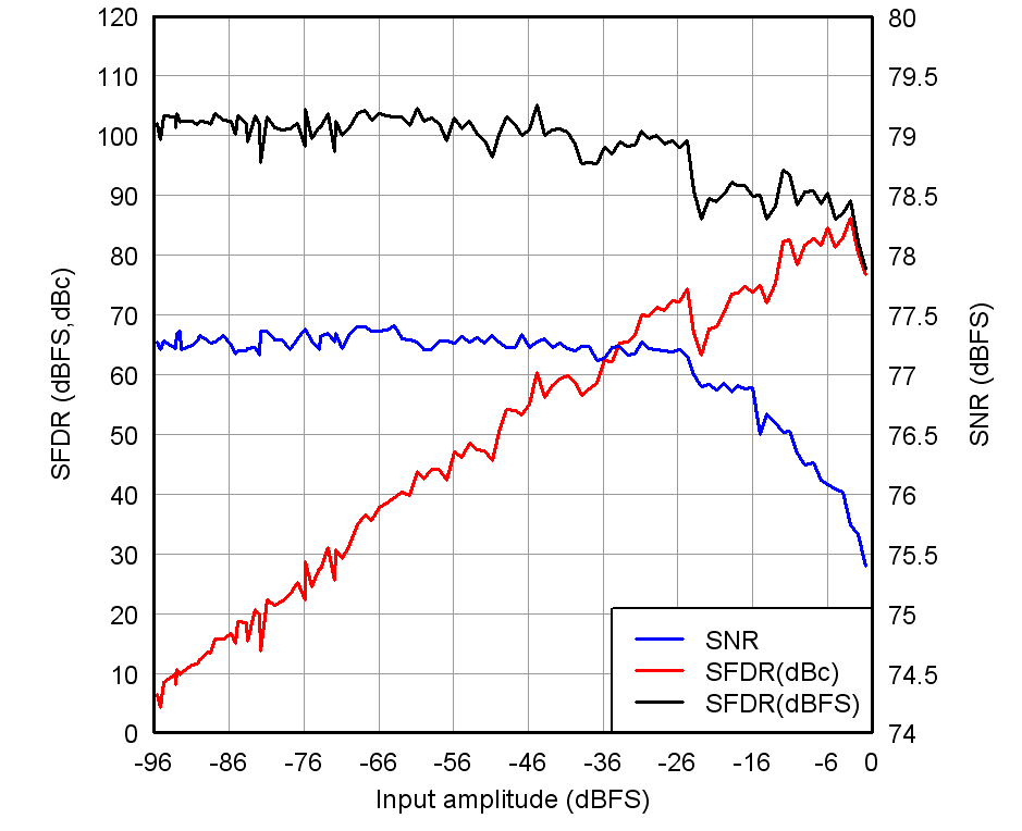 Figure 18. Performance vs Input Amplitude
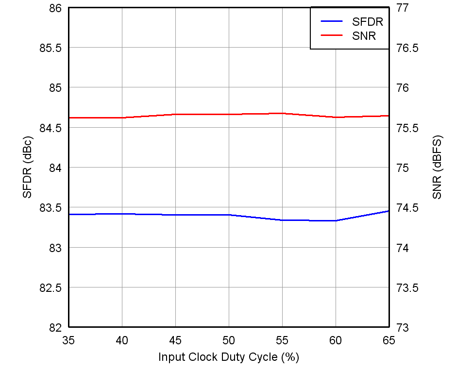 Figure 20. Performance vs Input Clock Duty CyclePerformance vs Input Clock Duty Cycle
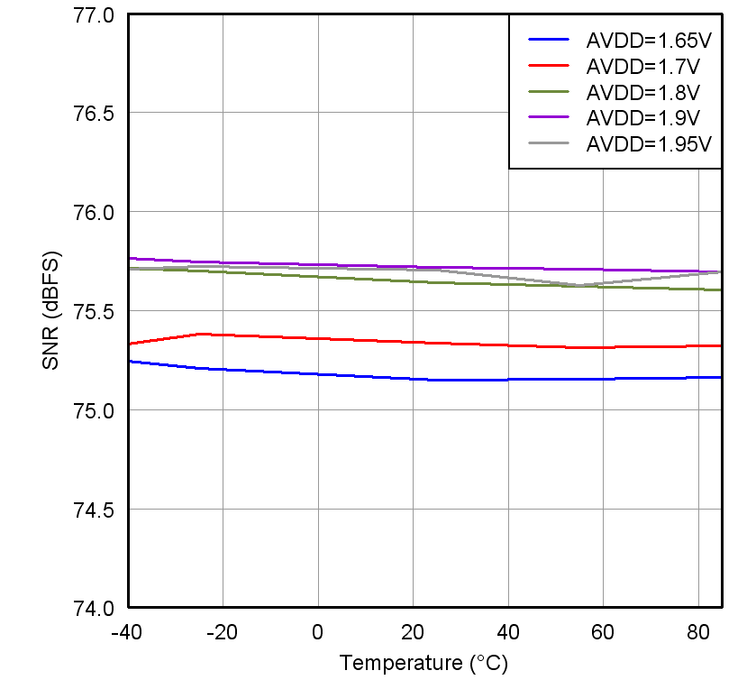 Figure 22. Signal-To-Noise Ratio vs Temperature
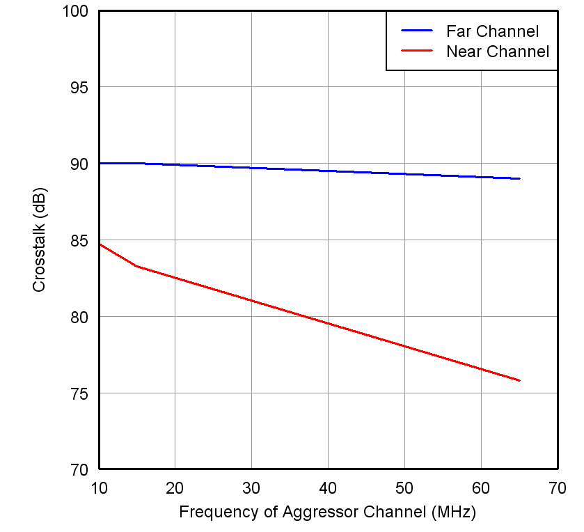 Figure 24. Crosstalk vs Frequency
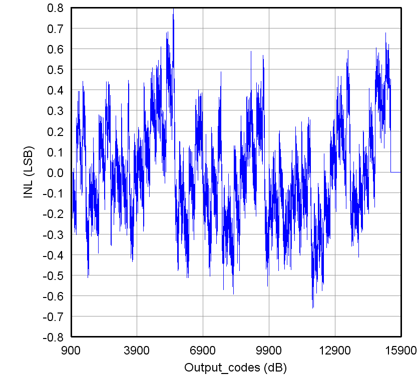 Figure 26. Integral Non-Linearity
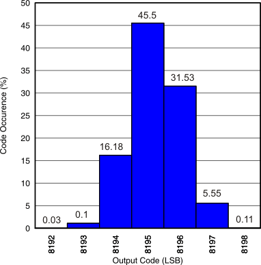 Figure 28. Histogram of Output Code With Analog Inputs Shorted (RMS Noise = 96.4 uV) a note "RMS Noise = 96.4 uV" to Figure 28
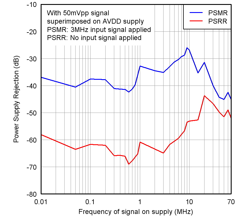 Figure 30. Power-Supply Rejection Ratio vs Frequency
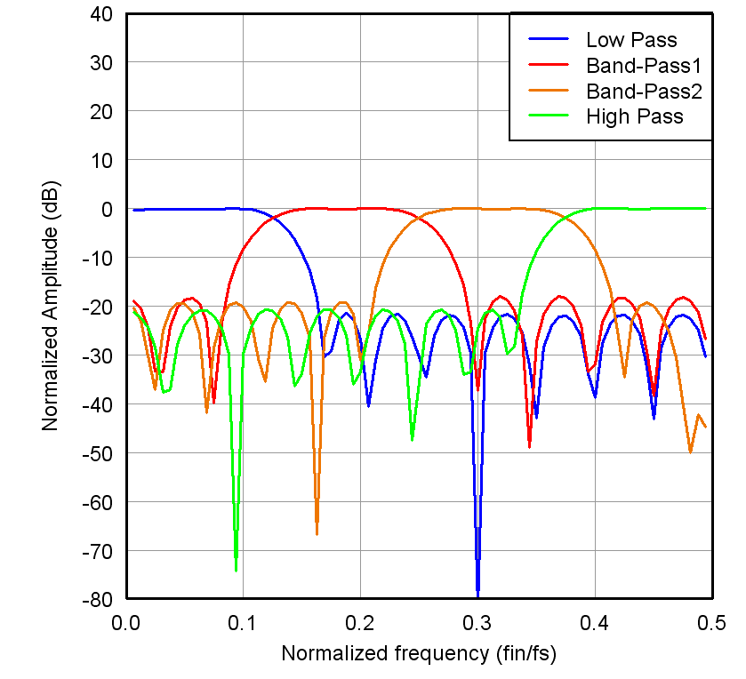 Figure 32. Filter Response, Decimate by 4
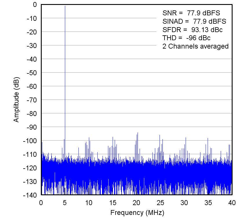 Figure 34. FFT for 5-MHz Input Signal, Sample Rate = 80 MSPS by Averaging 2 Channels
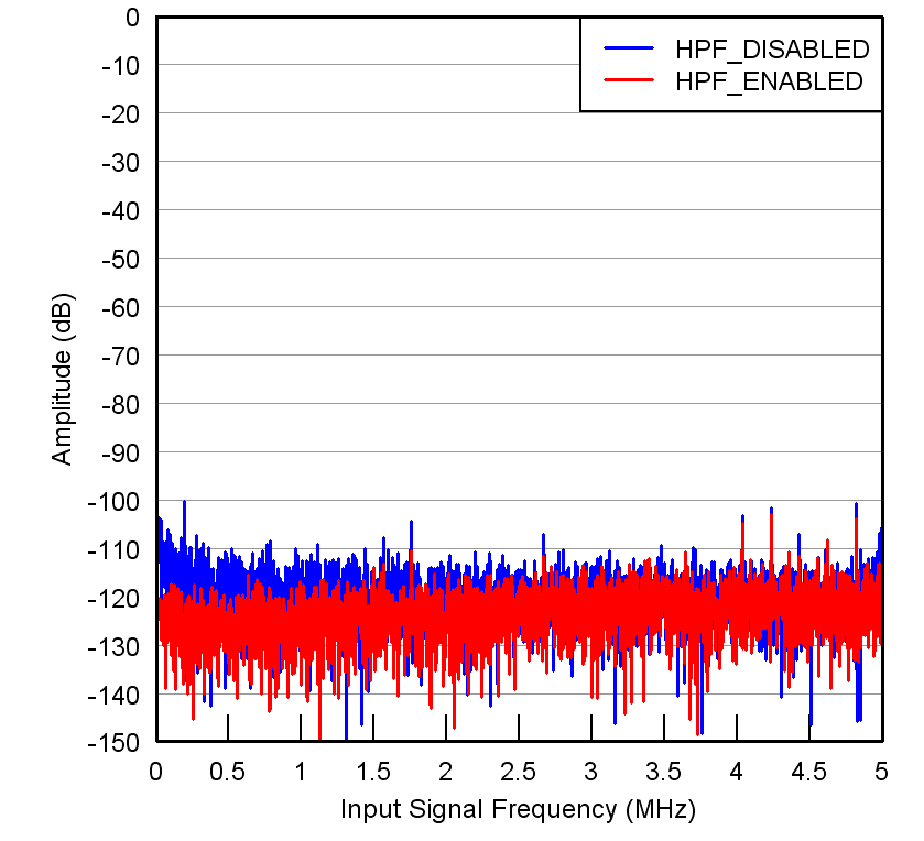 Figure 36. FFT with HPF Enabled and Disabled, No Signal
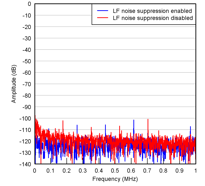 Figure 38. FFT (0 to 1 MHz) for 5-MHz Input Signal, Sample Rate = 80 MSPS with Low Frequency Noise Suppression Enabled
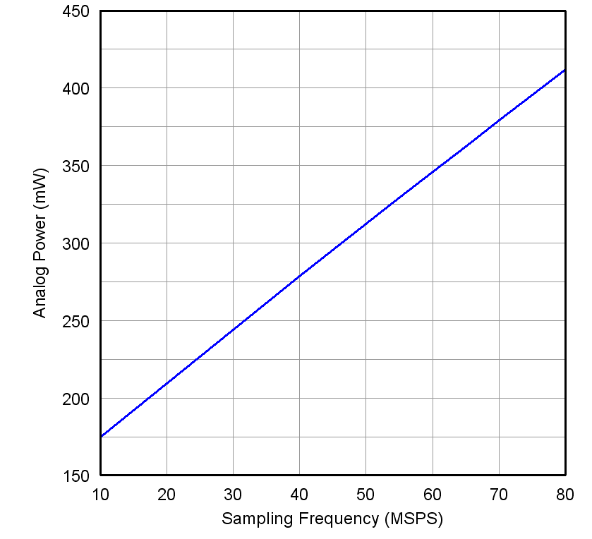 Figure 40. Power Consumption on Analog Supply
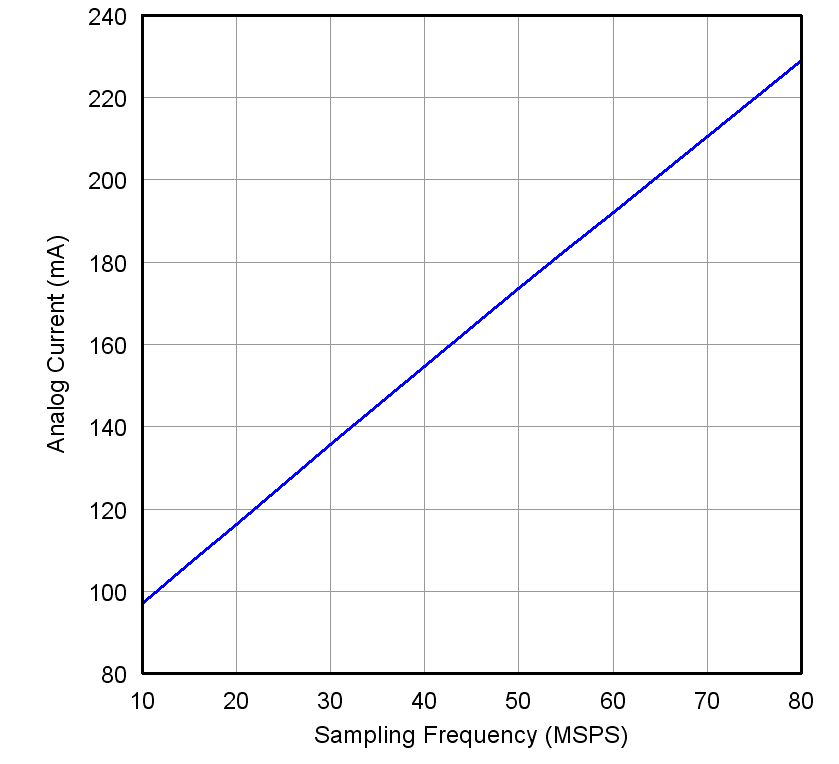 Figure 42. Supply Current on Analog Supply
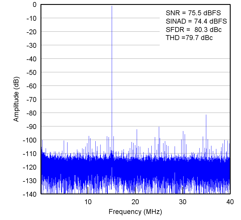 Figure 9. FFT for 15-MHz Input Signal, Sample Rate = 80 MSPS
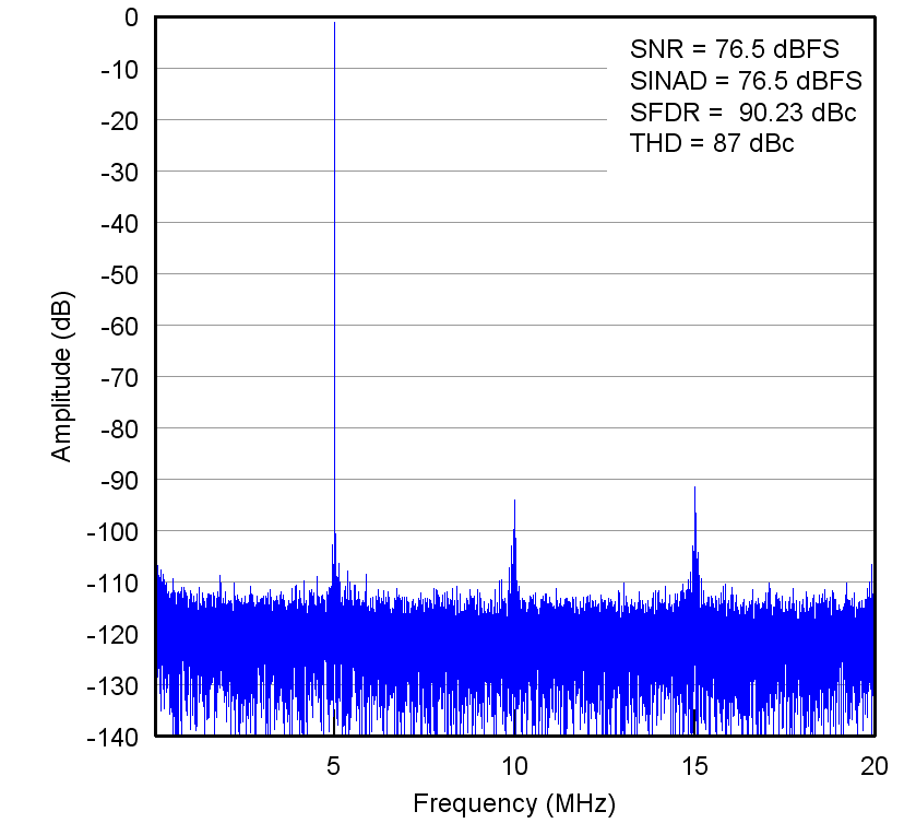 Figure 11. FFT for 5-MHz Input Signal, Sample Rate = 40 MSPS
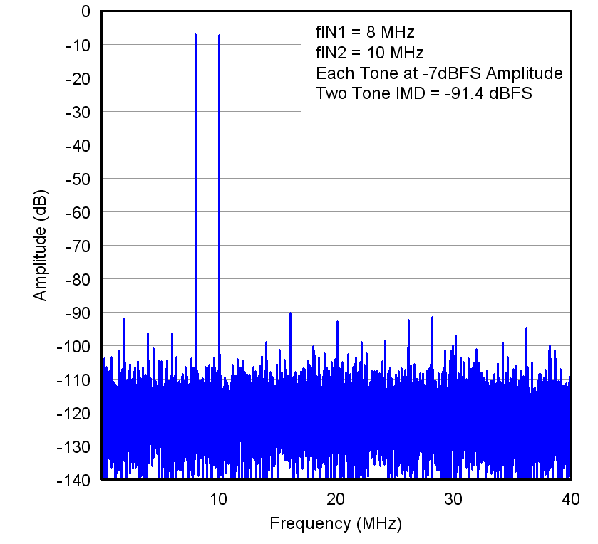 Figure 13. Two-Tone Intermodulation
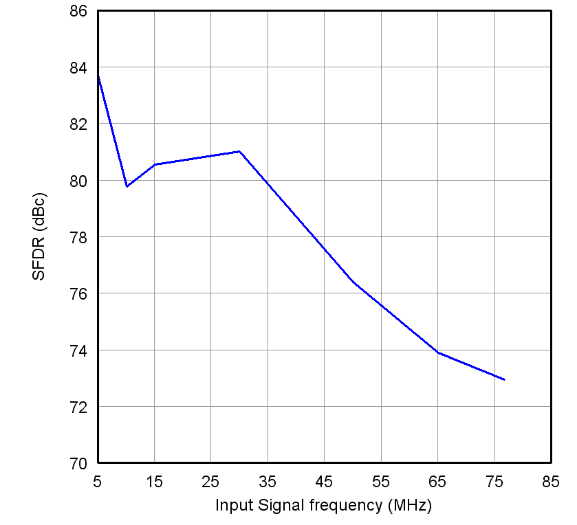 Figure 15. Spurious-Free Dynamic Range vs Input Signal Frequency
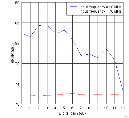 Figure 17. SFDR vs Digital Gain
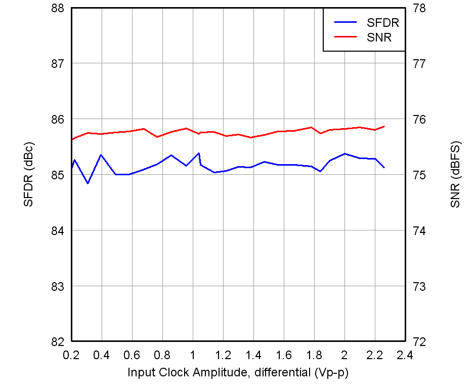 Figure 19. Performance vs Clock Input Amplitudes
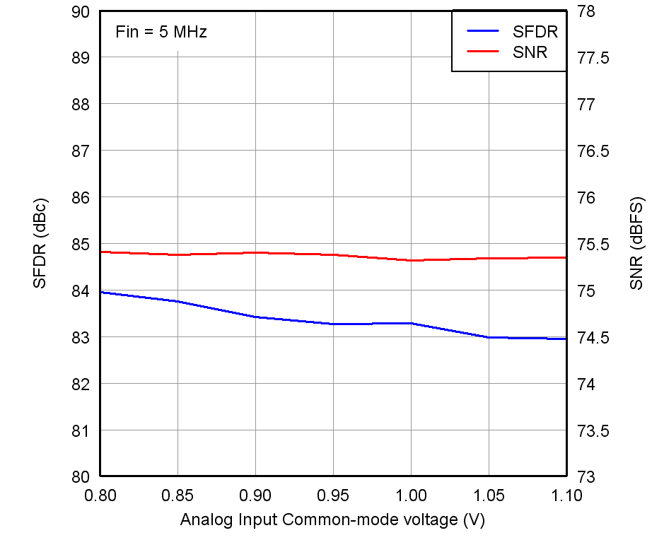 Figure 21. Performance vs Input VCM
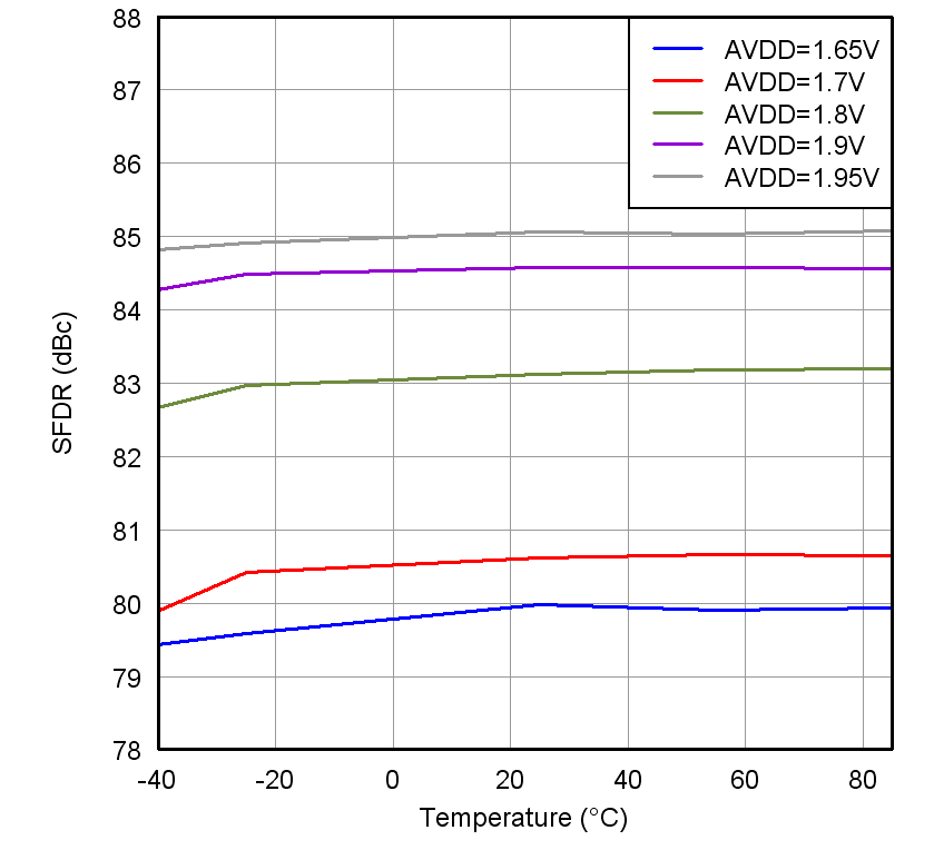 Figure 23. Spurious-Free Dynamic Range vs Temperature
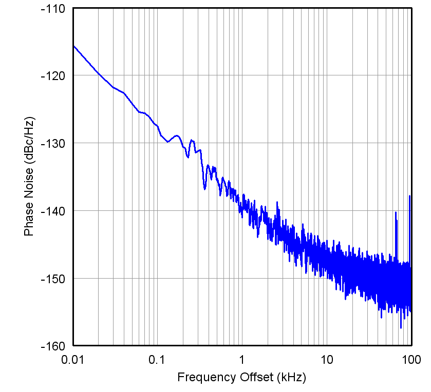 Figure 25. Phase Noise for 5-MHz Input Signal, Sample Rate = 80 MSPS
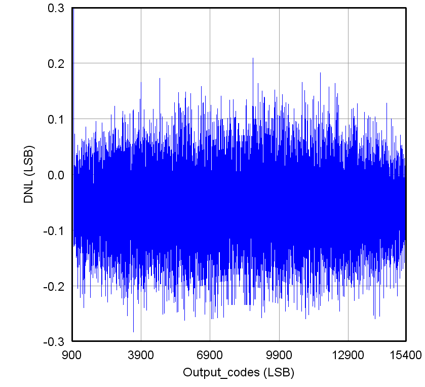 Figure 27. Differential Non-Linearity
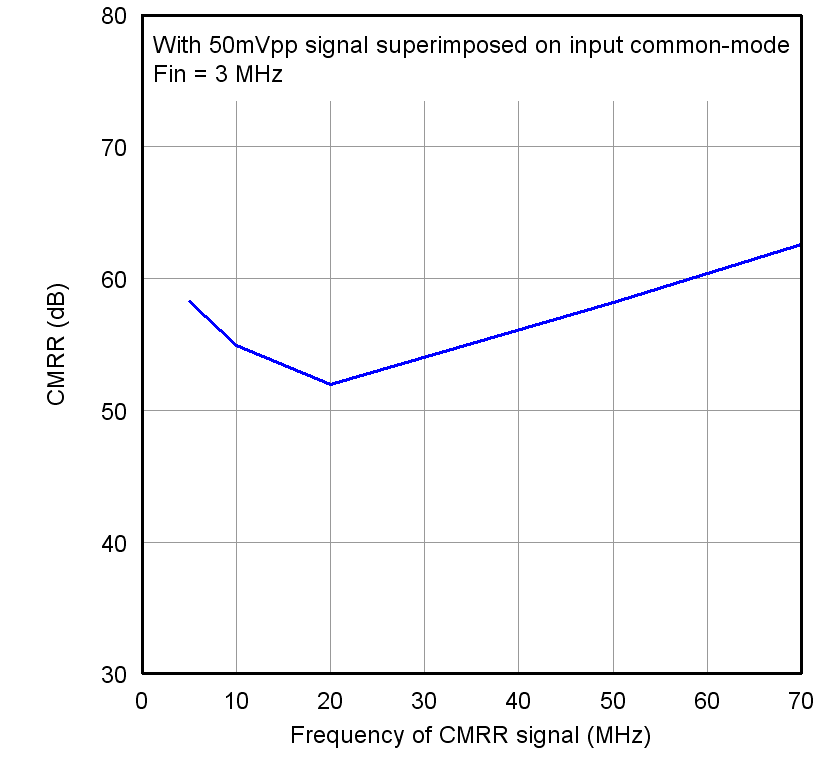 Figure 29. Common Mode Rejection Ratio vs Frequency
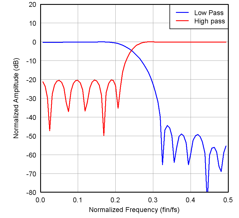 Figure 31. Filter Response, Decimate by 2
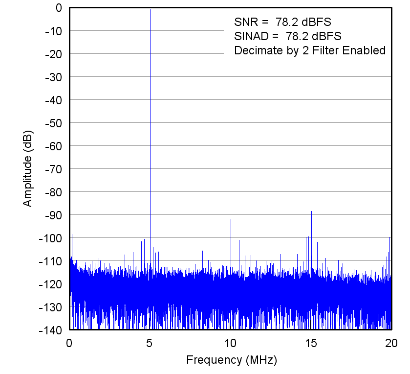 Figure 33. FFT for 5-MHz Input Signal, Sample Rate = 80 MSPS with Decimation Filter = 2
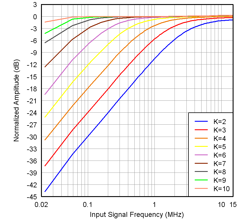 Figure 35. Digital High-Pass Filter Response
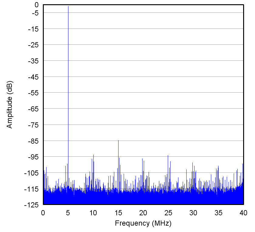 Figure 37. FFT (Full-Band) for 5-MHz Input Signal, Sample Rate = 80 MSPS with Low Frequency Noise Suppression Enabled
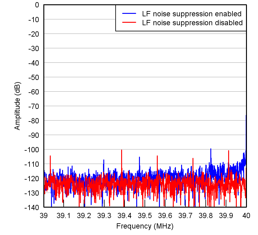 Figure 39. FFT (39 MHz to 40 MHz) for 5-MHz Input Signal, Sample Rate = 80 MSPS with Low Frequency Noise Suppression Enabled
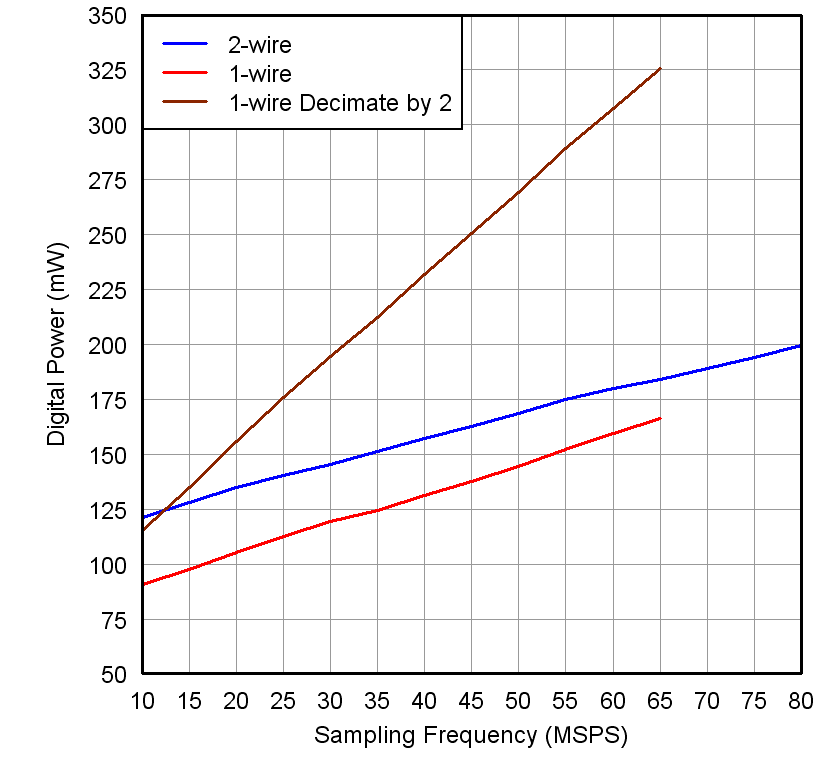 Figure 41. Power Consumption on Digital Supply
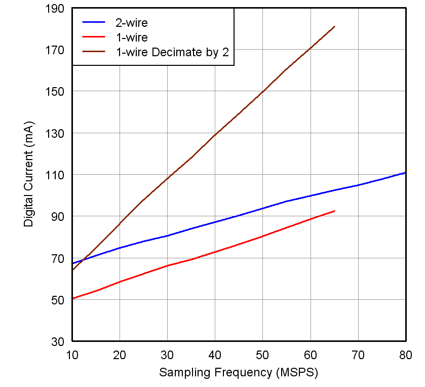 Figure 43. Supply Current on Digital Supply