Packaging information
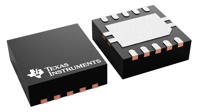
| Package | Pins VSON (DRC) | 10 |
| Operating temperature range (°C) -40 to 125 |
| Package qty | Carrier 3,000 | LARGE T&R |
Features for the LM5108
- Drives two N-channel MOSFETs in high-side low-side configuration
- Available in 3-mm x 3-mm package
- Interlock or cross-conduction protection
- Enable/disable functionality
- Absolute maximum negative voltage handling on HS (–7 V)
- 5-V typical under voltage lockout
- 20-ns typical propagation delay
- 11-ns rise, 8-ns typical fall time with 1000-pF load
- 1-ns typical delay matching
- 2.6-A sink, 1.6-A source output currents
- Absolute maximum boot voltage 110 V
- Low current (7-µA) consumption when disabled
- Integrated bootstrap diode
Description for the LM5108
The LM5108 is a high frequency half-bridge gate driver with maximum switch node (HS) voltage rating of 100 V. It allows for two N-channel MOSFETs to be controlled in half-bridge configuration based topologies such as synchronous buck, full bridge, active clamp forward, LLC, and synchronous boost.
The device has interlock functionality which, prevents both outputs from being high at the same time, in the case when both of the inputs are high. This interlock feature improves system robustness in motor drive and power tools applications. Enable and disable functionality allows for the flexible and fast control of the power stage. Battery powered tools can also use enable feature of the LM5108 to reduce the standby current as well as to respond to system fault. The inputs are independent of supply voltage and can have independent pulse width. This allows maximum control flexibility. Both inputs and enable have sufficient hysteresis to improve the system robustness in noise prone applications such as motor drives.
The low-side and the high-side outputs are matched to 1-ns between the turn-on and turn-off of each other. This allows for dead-time optimization which in-turn improves efficiency. 5-V UVLO allows the driver to operate at lower bias supplies which further allows the power stage to operate at higher switching frequency without increasing switching losses. VDD and HB UVLO threshold specifications are designed in such as way that both the high-side and low-side driver turns on typically at 5 V. If both VDD and HB UVLO thresholds are the same then designer would need higher bias supply than the VDD UVLO threshold to turn-on both high-side and low-side driver.
An on-board bootstrap diode eliminates the need for an external discrete diode which improves board space utilization. Small package enables dense power designs such as power tools.