Packaging information
| Package | Pins SOT-23 (DBV) | 6 |
| Operating temperature range (°C) -40 to 105 |
| Package qty | Carrier 3,000 | LARGE T&R |
Features for the TPS22918-Q1
- AEC-Q100 Qualified
- Integrated single-channel load switch
- Qualified for automotive applications:
- Device Temperature Grade 2: –40°C to +105°C ambient operating temperature range
- Functional safety
capable
- Documentation available to aid functional safety system design
- Input voltage range: 1 V to 5.5 V
- Low On-Resistance
(RON)
- RON = 52 mΩ (typical) at VIN = 5 V
- RON = 53 mΩ (typical) at VIN = 3.3 V
- 2-A Maximum continuous switch current
- Low quiescent current
- 8.3 µA (typical) at VIN = 3.3 V
- Low-control input-threshold enables use of 1 V or higher GPIO
- Configurable Quick-Output Discharge (QOD)
- Configurable rise time with CT pin
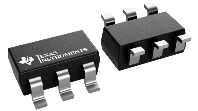
- Small SOT23-6 package (DBV)
- 2.9 mm × 2.8 mm, 0.95-mm Pitch,
1.45-mm height (with leads)
- 2.9 mm × 2.8 mm, 0.95-mm Pitch,
- ESD Performance tested per AEC Q100
- ±2-kV HBM and ±750-V CDM
Description for the TPS22918-Q1
The TPS22918-Q1 is a single-channel load switch with both configurable rise time and
configurable quick-output discharge. The device contains an N-channel MOSFET that can operate over
an input voltage range of 1 V to 5.5 V and can support a maximum continuous current of
2 A. The switch is controlled by an on and off input, which is capable of interfacing
directly with low-voltage control signals.
The configurable rise time of the device reduces inrush current caused by large bulk load capacitances, thereby reducing or eliminating power supply droop. The TPS22918-Q1 features a configurable quick output discharge (QOD) pin, which controls the fall time of the device to allow design flexibility for power down and sequencing.
The TPS22918-Q1 is available in a small, leaded SOT-23 package (DBV) which allows to visually inspect solder joints. The device is characterized for operation over the free-air temperature range of –40°C to +105°C.