SLUA887A August 2018 – September 2023 LM2005 , LM2101 , LM2103 , LM2104 , LM2105 , LM25101 , LM27222 , LM2724A , LM5100A , LM5100B , LM5100C , LM5101 , LM5101A , LM5101B , LM5101C , LM5102 , LM5104 , LM5105 , LM5106 , LM5107 , LM5108 , LM5109 , LM5109A , LM5109B , LM5109B-Q1 , LM5113-Q1 , LMG1205 , LMG1210 , SM72295 , SM74104 , TPS28225 , TPS28225-Q1 , TPS28226 , TPS2832 , TPS2836 , TPS2837 , UC2950 , UCC27200 , UCC27200-Q1 , UCC27200A , UCC27201 , UCC27201A , UCC27201A-DIE , UCC27201A-Q1 , UCC27211 , UCC27211A , UCC27211A-Q1 , UCC27212 , UCC27212A-Q1 , UCC27222 , UCC27282 , UCC27282-Q1 , UCC27284 , UCC27284-Q1 , UCC27288 , UCC27289 , UCC27301A , UCC27301A-Q1 , UCC27302A , UCC27302A-Q1 , UCC27311A , UCC27311A-Q1 , UCC27710 , UCC27712 , UCC27712-Q1 , UCC27714 , UCC27734 , UCC27734-Q1 , UCC27735 , UCC27735-Q1 , UCC27834 , UCC27834-Q1 , UCC27884 , UCC27884-Q1
4 Layout Considerations for Bootstrap Components
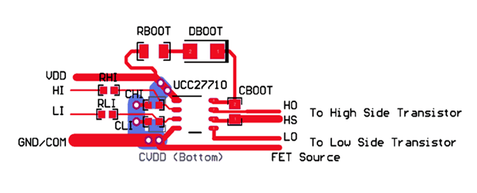
Once all bootstrap components appropriately selected, it is important to carefully place these components in order to minimize parasitic inductances and reduce high current trace length. This high current path includes the bootstrap capacitor, the bootstrap diode, the ground-referenced VDD bypass capacitor of the driver, and the low-side power switch. It is therefore important to reduce that path and keep that loop as small as possible. The bootstrap capacitor and bypass capacitor should be placed as closed as possible to the gate driver supply pins. Figure 4-1 below shows a good layout example using UCC27710 with all bootstrap components located near the gate driver IC minimizing any effects of parasitic inductances and reducing the high peak currents path of the bootstrap circuit. It is also important to separate high voltage power and low voltage signal traces.
 Figure 4-1 Layout Example using UCC27710