SPRUIX0D February 2021 – August 2021
- Trademarks
- 1Introduction
- 2Important Usage Notes
-
3System Description
- 3.1 Key Features
- 3.2 Functional Block Diagram
- 3.3 Power-On/Off Procedures
- 3.4
Peripheral and Major Component
Description
- 3.4.1 Clocking
- 3.4.2 Reset
- 3.4.3 Power
- 3.4.4 Configuration
- 3.4.5 JTAG
- 3.4.6 Test Automation
- 3.4.7 UART Interfaces
- 3.4.8 Memory Interfaces
- 3.4.9 Ethernet Interface
- 3.4.10 Display Interface
- 3.4.11 USB 2.0 Interface
- 3.4.12 PCIe Interface
- 3.4.13 High Speed Expansion Interface
- 3.4.14 CAN Interface
- 3.4.15 Interrupt
- 3.4.16 ADC Interface
- 3.4.17 Safety Connector
- 3.4.18 SPI Interfaces
- 3.4.19 I2C Interfaces
- 3.4.20 FSI Interface
- 4Known Issues and Modifications
- 5References
- 6Revision History
3.4.12 PCIe Interface
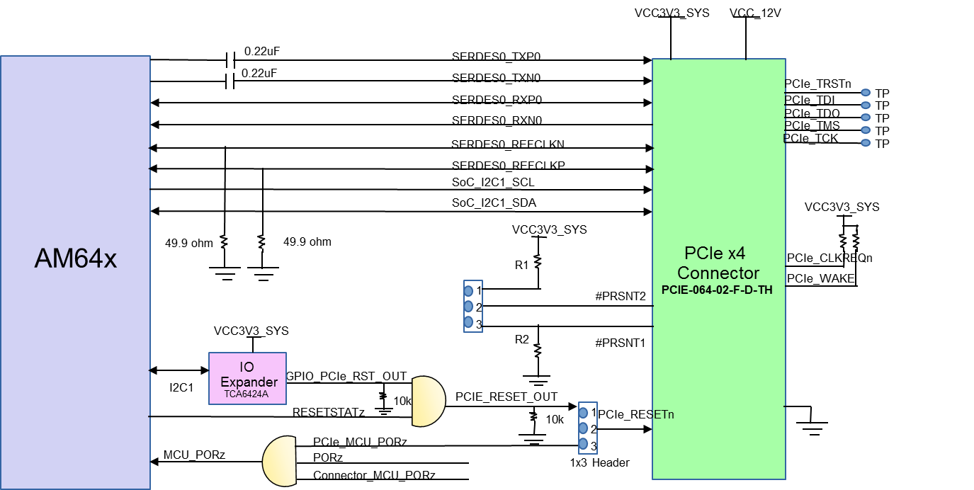
The Serdes0 interface of AM64x/AM243x is used to implement a x1 lane PCIe interface with the signals routed to a x4 PCIe slot connector. PCIE-064-02-F-D-TH connector from Samtec is be used for the PCIe interface and this connector meets the PCIe CEM v2.0 specification both physically and electrically and it is designed to support a 25W slot including 2.1A for the 12 V rail and 3A for the 3.3 V rail. The PCIe interface is designed to support either root complex operation or endpoint operation with a cross over cable. SoC_I2C1 is used for control purpose. The link activation signal from PCIe connectors is pulled up to VCC3V3_SYS.
Clock: SERDES REFCLK is routed to the PCIe REF CLK pins to allow either receiving or providing a clock from the connector (no separate PLL to generate PCIe REF CLK available on the EVM).
Hot plug: The PRSNT1# and PRSNT2# signals are the hot plug presence detect signals. The PRSNT2# is pulled up and PRSNT1# is connected to ground so that PRSNT2# will be pulled low when a daughter card is plugged in. A 3 pin header (J35) is provided to choose between RC and EP mode.
Reset: A 3 pin header (J34) is provided to select the reset source for host and endpoint PCIe operation. In case of host mode, PCIe_RST_OUT signal from IO Expander and RESETSTATz signal from SoC are ANDed and the output is connected to PCIe connector through 3 pin header. A jumper is mounted for the connectivity. Whereas in case of PCIe end point operation, the AM64x SoC receives reset signal from the add-on card and passed on to the MCU_PORz pin. The reset signal is connected to 3 pin header and the selection should be made with a jumper.
The PCIe x4 Connector JTAG signals are unused and test points are provided on the signals.
Table 3-22 describes the jumper options used to select if the GP EVM will operate in Root Complex mode or in End Point mode.
| Root Complex | End Point | |
|---|---|---|
| 1x3 header J34 and J35 | Short 1 and 2 | Short 2 and 3 |
 Figure 3-25 AM64x/AM243x PCIe Interface
| Pin No. | Side A of PCIe Connector | GP Board Signal | Side B of PCIe Connector | GP Board Signal |
|---|---|---|---|---|
| 1 | PRSNT1# | J35.3 | +12V | VDD_12V |
| 2 | +12V | VDD_12V | +12V | VDD_12V |
| 3 | +12V | VDD_12V | +12V | VDD_12V |
| 4 | GND | GROUND | GND | GROUND |
| 5 | JTAG2 | TP | SMCLK | SoC_I2C1_CLK |
| 6 | JTAG3 | TP | SMDATA | SoC_I2C1_SDA |
| 7 | JTAG4 | TP | GND | GROUND |
| 8 | JTAG5 | TP | +3V3 | VCC3V3_SYS |
| 9 | +3V3 | VCC3V3_SYS | JTAG1 | TP |
| 10 | +3V3 | VCC3V3_SYS | 3V3 VAUX | VCC3V3_SYS |
| 11 | PERST# | J24.2 | WAKE# | Pulled up to VCC3V3_SYS |
| 12 | GND | GROUND | RSVD4 | Pulled up to VCC3V3_SYS |
| 13 | REFCLK+ | SERDES_REFCLK0P | GND | GROUND |
| 14 | REFCLK- | SERDER_REFCLK0N | PETp0 | SERDES_TXP0 |
| 15 | GND | GROUND | PETn0 | SERDES_TXN0 |
| 16 | PERp0 | SERDES_RXP0 | GND | GND |
| 17 | PERn0 | SERDES_RXN0 | PRSNT2#_1 | J35.2 |
| 18 | GND | GROUND | GND | GROUND |
| 19 | RSVD1 | NC | PETp1 | NC |
| 20 | GND | GROUND | PETn1 | NC |
| 21 | PERp1 | NC | GND | GROUND |
| 22 | PERn1 | NC | GND | GROUND |
| 23 | GND | GROUND | PETp2 | NC |
| 24 | GND | GROUND | PETn2 | NC |
| 25 | PERp2 | NC | GND | GROUND |
| 26 | PERn2 | NC | GND | GROUND |
| 27 | GND | GROUND | PETp3 | NC |
| 28 | GND | GROUND | PETn3 | NC |
| 29 | PERp3 | NC | GND | GROUND |
| 30 | PERn3 | NC | RSVD3 | NC |
| 31 | GND | GROUND | PRSNT2#_2 | NC |
| 32 | RSVD2 | NC | GND | GROUND |