SPRUIX0D February 2021 – August 2021
- Trademarks
- 1Introduction
- 2Important Usage Notes
-
3System Description
- 3.1 Key Features
- 3.2 Functional Block Diagram
- 3.3 Power-On/Off Procedures
- 3.4
Peripheral and Major Component
Description
- 3.4.1 Clocking
- 3.4.2 Reset
- 3.4.3 Power
- 3.4.4 Configuration
- 3.4.5 JTAG
- 3.4.6 Test Automation
- 3.4.7 UART Interfaces
- 3.4.8 Memory Interfaces
- 3.4.9 Ethernet Interface
- 3.4.10 Display Interface
- 3.4.11 USB 2.0 Interface
- 3.4.12 PCIe Interface
- 3.4.13 High Speed Expansion Interface
- 3.4.14 CAN Interface
- 3.4.15 Interrupt
- 3.4.16 ADC Interface
- 3.4.17 Safety Connector
- 3.4.18 SPI Interfaces
- 3.4.19 I2C Interfaces
- 3.4.20 FSI Interface
- 4Known Issues and Modifications
- 5References
- 6Revision History
3.4.5 JTAG
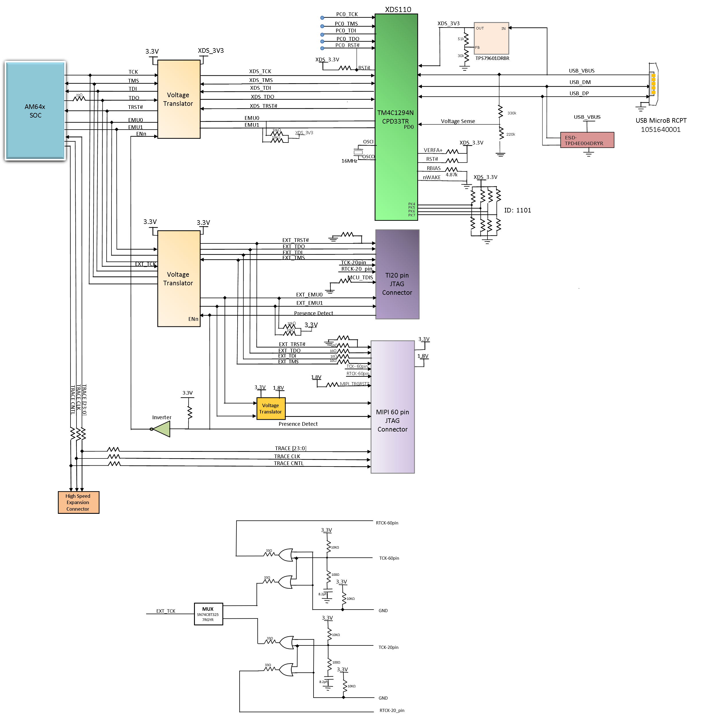
The GP EVM includes XDS110 class embedded JTAG emulation through the micro B connector J28. It also has an optional TI20 pin (J25) connector to support external JTAG emulation. When an external emulator is connected, internal emulation circuitry will be disabled.
The design includes the footprint for a MIPI60 (J33) connector with connections for JTAG and trace capabilities. The trace pins are pinmuxed with GPMC signals which, by default, are connected to HSE connector on the processor board. Resistor networks are used to steer these signals to either the HSE connector or to the MIPI60 connector. The MIPI60 is not installed as delivered.
Resistor options are provided to connect these signals to the HSE or Trace connector as mentioned in the Table 3-13.
The pinout of TI20 pin connector and MIPI60 pin connector are given in Table 3-13 and Table 3-15, respectively.
| Signals Selected | Mount | Un Mount |
|---|---|---|
|
HSE Connector (default) |
RA1 | RA2 |
| RA3 | RA4 | |
| RA5 | RA6 | |
| R390 | R391 | |
| R393 | R392 | |
| JTAG Trace signals to J33 | RA2 | RA1 |
| RA4 | RA3 | |
| RA6 | RA5 | |
| R391 | R390 | |
| R392 | R393 |
| Pin No. | Signal | Pin No. | Signal |
|---|---|---|---|
| 1 | JTAG_CTI_TMS | 11 | JTAG_CTI_TCK |
| 2 | JTAG_TRSTN | 12 | DGND |
| 3 | JTAG_CTI_TDI | 13 | JTAG_EMU0 |
| 4 | JTAG_TDIS | 14 | JTAG_EMU1 |
| 5 | VCC_3V3_SYS | 15 | JTAG_EMU_RSTN |
| 6 | NC | 16 | DGND |
| 7 | JTAG_TDO | 17 | NC |
| 8 | SEL_XDS110_INV | 18 | NC |
| 9 | JTAG_CTI_RTCK | 19 | NC |
| 10 | DGND | 20 | DGND |
 Figure 3-11 JTAG Interface
| Pin No. | Signal | Pin No. | Signal |
|---|---|---|---|
| 1 | VCC3V3_R | 31 | MIPI_TRC_DAT06 |
| 2 | MIPI_TMS_R | 32 | NC |
| 3 | JTAG_MIPI_TCK | 33 | MIPI_TRC_DAT07 |
| 4 | MIPI_TDO_R | 34 | NC |
| 5 | MIPI_TDI_R | 35 | MIPI_TRC_DAT08 |
| 6 | MIPI_EMU_RSTn | 36 | NC |
| 7 | MIPI_RTCK | 37 | MIPI_TRC_DAT09 |
| 8 | MIPI_TRST#_R | 38 | JTAG_MIPI_EMU0 |
| 9 | NC | 39 | MIPI_TRC_DAT10 |
| 10 | NC | 40 | JTAG_MIPI_EMU1 |
| 11 | NC | 41 | MIPI_TRC_DAT11 |
| 12 | VCC_3V3_MIPI | 42 | NC |
| 13 | MIPI_TRC_CLK | 43 | MIPI_TRC_DAT12 |
| 14 | NC | 44 | NC |
| 15 | DGND | 45 | MIPI_TRC_DAT13 |
| 16 | DGND | 46 | NC |
| 17 | MIPI_TRC_CTL | 47 | MIPI_TRC_DAT14 |
| 18 | MIPI_TRC_DAT19 | 48 | NC |
| 19 | MIPI_TRC_DAT00 | 49 | MIPI_TRC_DAT15 |
| 20 | MIPI_TRC_DAT20 | 50 | NC |
| 21 | MIPI_TRC_DAT01 | 51 | MIPI_TRC_DAT16 |
| 22 | MIPI_TRC_DAT21 | 52 | NC |
| 23 | MIPI_TRC_DAT02 | 53 | MIPI_TRC_DAT17 |
| 24 | MIPI_TRC_DAT22 | 54 | NC |
| 25 | MIPI_TRC_DAT03 | 55 | MIPI_TRC_DAT18 |
| 26 | MIPI_TRC_DAT23 | 56 | NC |
| 27 | MIPI_TRC_DAT04 | 57 | DGND |
| 28 | NC | 58 | SEL_XDS100_INV |
| 29 | MIPI_TRC_DAT05 | 59 | NC |
| 30 | NC | 60 | NC |