SPRUIX0D February 2021 – August 2021
- Trademarks
- 1Introduction
- 2Important Usage Notes
-
3System Description
- 3.1 Key Features
- 3.2 Functional Block Diagram
- 3.3 Power-On/Off Procedures
- 3.4
Peripheral and Major Component
Description
- 3.4.1 Clocking
- 3.4.2 Reset
- 3.4.3 Power
- 3.4.4 Configuration
- 3.4.5 JTAG
- 3.4.6 Test Automation
- 3.4.7 UART Interfaces
- 3.4.8 Memory Interfaces
- 3.4.9 Ethernet Interface
- 3.4.10 Display Interface
- 3.4.11 USB 2.0 Interface
- 3.4.12 PCIe Interface
- 3.4.13 High Speed Expansion Interface
- 3.4.14 CAN Interface
- 3.4.15 Interrupt
- 3.4.16 ADC Interface
- 3.4.17 Safety Connector
- 3.4.18 SPI Interfaces
- 3.4.19 I2C Interfaces
- 3.4.20 FSI Interface
- 4Known Issues and Modifications
- 5References
- 6Revision History
3.4.19 I2C Interfaces
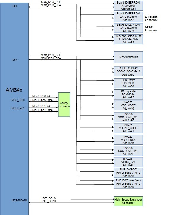
There are five I2C interfaces used in the GP EVM board.
- MAIN_I2C0: This interface is used by
the software to identify the EVM and to control the power supply circuit. It is
interfaced to presence detect latch to identify the daughter cards which are presently
installed, Board ID memory device, board ID memories of the daughter cards and HSE
connector. This I2C is also connected to a test header J5 for AM64x/AM243x processor slave operation. Pin outs of I2C test header is given in
Table 3-28.Table 3-28 I2C Test Header (J5) Pin-out
Pin No. Signal 1 DGND 2 SoC_I2C0_SDA 3 SoC_I2C0_SCL - MAIN_I2C1:
This is interfaced to 16 bit GPIO expanders that is being used for all control signals
and LED controls, 8bit LED Driver with part number TPIC2810, Current Monitors
with part number INA226 to monitor current of VDD_CORE, VDDAR_CORE, SoC_DVDD3V3,
SoC_DVDD1V8, VDDA_1V8, VDD_DDR4 , Temperature sensor with part number TMP100,
Display Interface with part number OSD9616P0992-10, Test automation connector via
voltage isolation. This I2C is also connected to a test header J4 for AM64x processor
slave operation. Pin outs of I2C test header is given in Table 3-29.Table 3-29 I2C Test Header (J4) Pin-out
Pin No. Signal 1 SoC_I2C1_SCL 2 SoC_I2C0_SDA 3 DGND 4 INA_ALERT 5 NC - MAIN_I2C3: This is connected to the expansion board connector from a mux. I2C3 is muxed with the MCAN signals. The default state of the mux is MCAN.
- MCU_I2C0: This is connected to the safety connector.
- MCU_I2C1: This is connected to the safety connector.
Figure 3-30 depicts the I2C tree.
 Figure 3-30 AM64x/AM243x I2C Interfaces and Address Assignment of Peripherals